Renesas RA Family RA4 Quick Design Guide
R01AN5988EU0100 Rev.1.00 Page 18 of 51
Jul.21.21
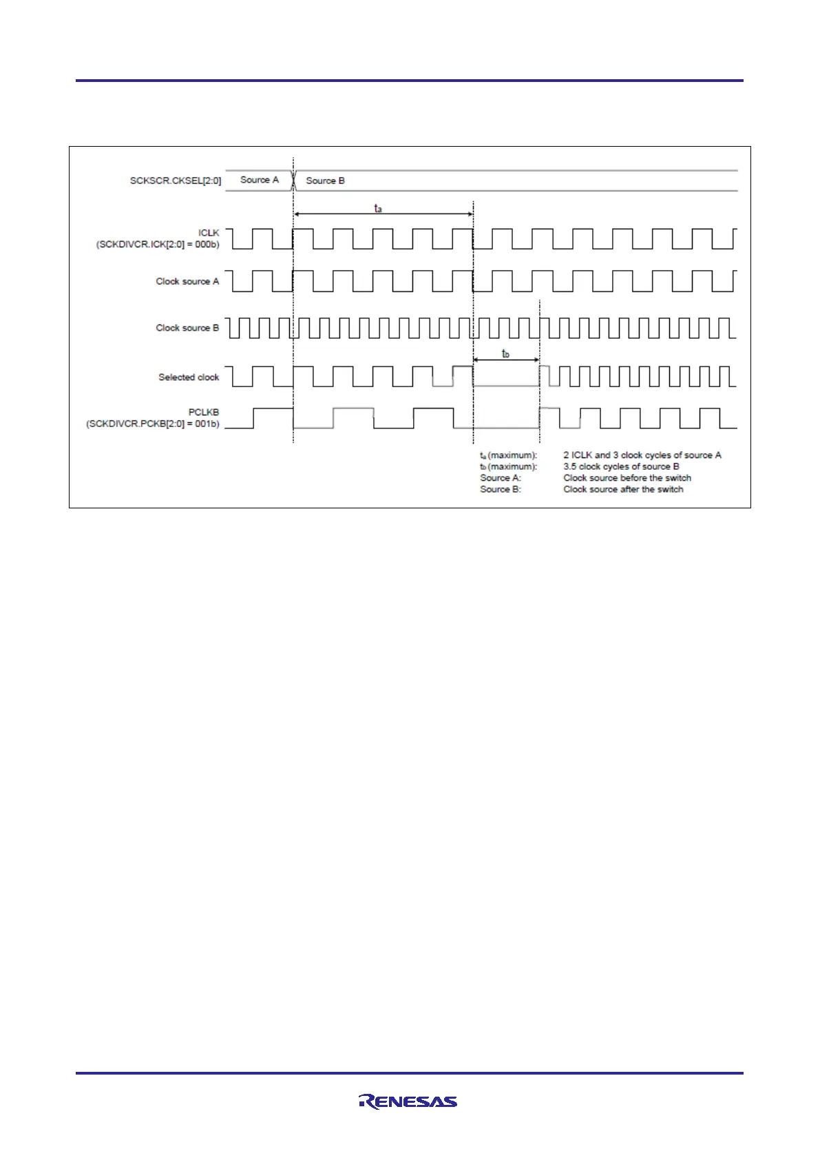
To ensure correct processing after the clock frequency changes, first write to the relevant Clock Control
register to change the frequency, then read the value from the register, and finally perform the subsequent
processing.
Figure 11. Timing of Clock Source Switching
5.5 Clock Setup Example
Renesas FSP provides a simple, visual clock configuration tool for RA4M3 MCU shown as follows.

 Loading...


