Renesas RA Family RA4 Quick Design Guide
R01AN5988EU0100 Rev.1.00 Page 31 of 51
Jul.21.21
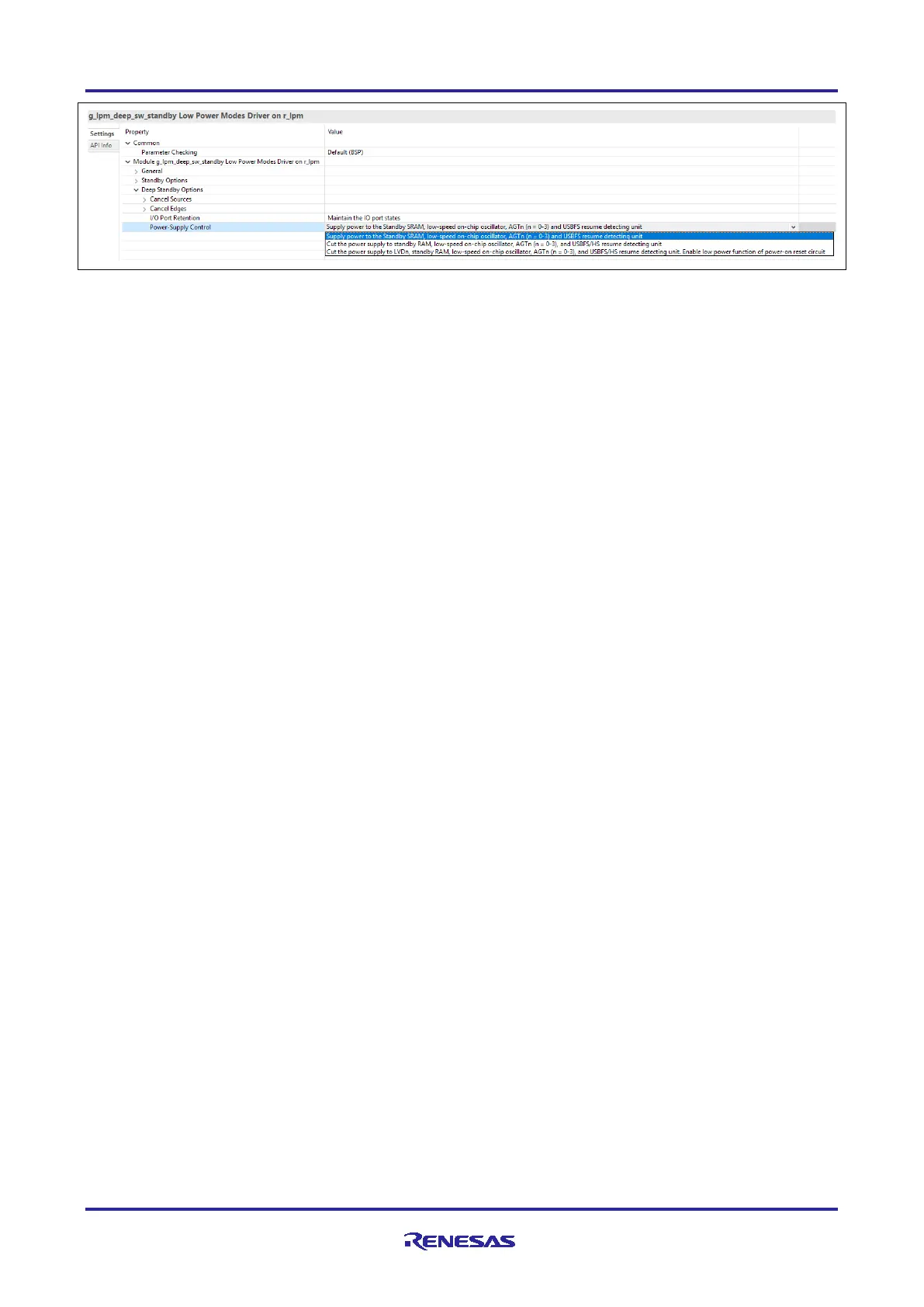
Figure 23. Enable/Disable Power Supply to Standby SRAM Using Renesas FSP Configurator
8.3 Peripheral I/O Registers
Blocks of peripheral I/O registers appear at various locations in the memory map depending on the device
and the current operating mode. The majority of peripheral I/O registers occupy a region from address
4000 0000h to 400F FFFFh. However, this may vary in location and size by device. Consult the Hardware
User’s Manual for specifics. Details can be found in the “I/O Registers” appendix, and also in the register
descriptions for each peripheral function. This region contains registers that are available at all times in all
modes of operation. Flash I/O registers to control access flash memory occupy two regions, 407E 0000h to
407E FFFFh and 407F C000h to 407F FFFFh.
The Renesas FSP provides C header files in CMSIS data structure that map all of the peripheral I/O
registers for a specific device to easily accessible I/O data structures.
8.4 On-Chip Flash Memory
The RA4 MCUs feature two flash memory sections, code flash and data flash, which vary in size and
programmable cycle capacity by device. The Flash Control Unit (FCU) controls programming and erasure of
the flash memory. The Flash Application Command Interface (FACI) controls the FCU in accordance with the
specified FACI commands.
The code flash is designed to store user application code and constant data. The data flash is designed to
store information that may be updated from time to time such as configuration parameters, user settings, or
logged data. The units of programming and erasure in the data flash area are much smaller than that of the
code flash (2 bytes for data flash versus 128 bytes for code flash).
Both the data flash and code flash areas can be programmed or erased by application code. This enables
field firmware updates without having to connect an external programming tool.
Renesas FSP provides HAL layer drivers for both code flash memory and data flash memory.
The following figure shows example specifications of code flash memory and data flash memory.

 Loading...


