Renesas RA Family RA4 Quick Design Guide
R01AN5988EU0100 Rev.1.00 Page 17 of 51
Jul.21.21
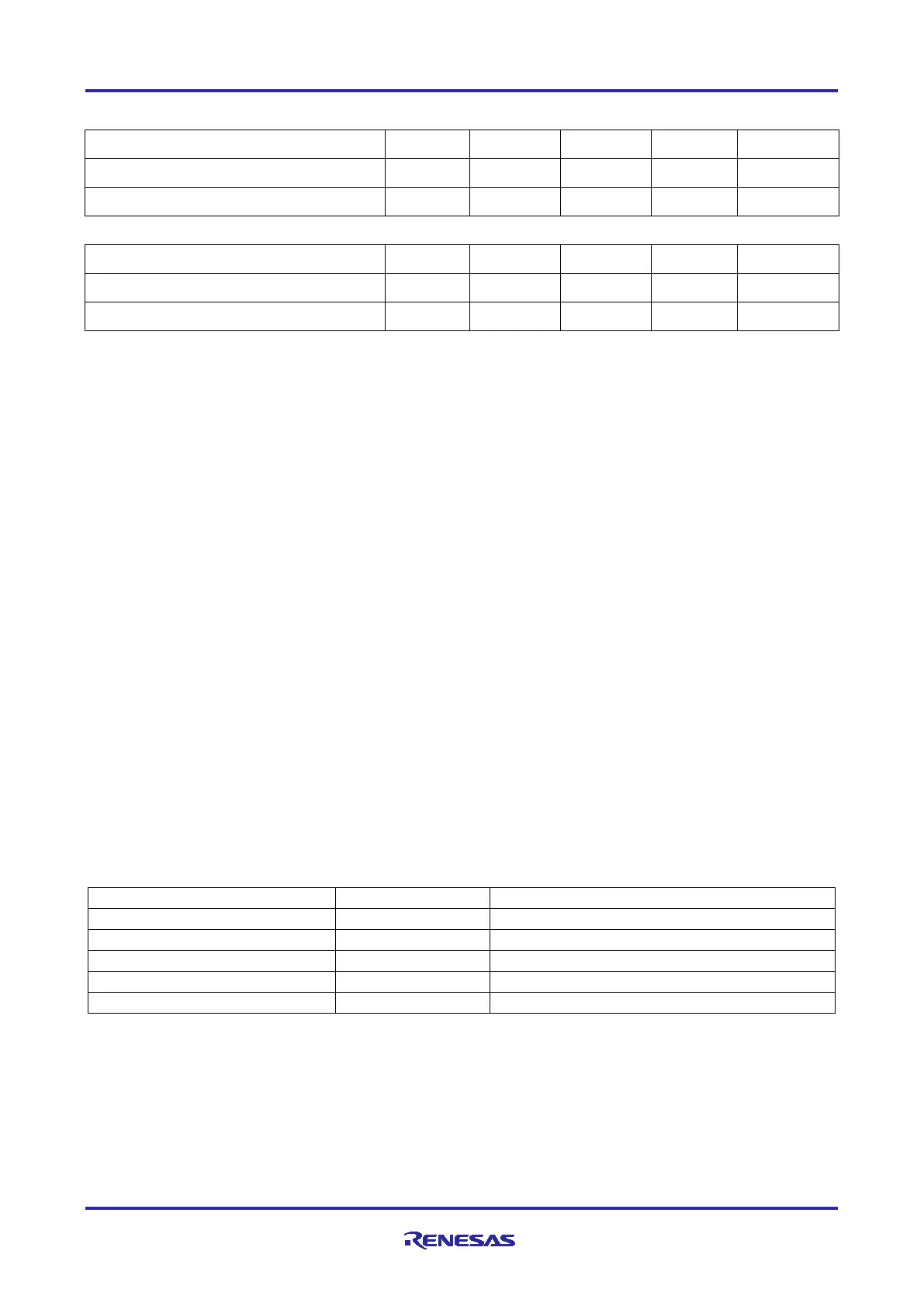
Table 9. Frequency Range for Arm Cortex-M33 MCU Internal Clocks
Note 1. The FCLK must run at a frequency of at least 4 MHz when writing or erasing ROM or data flash.
5.2.1 Requirements for USB Communications
The USB 2.0 Full-Speed Module (USBFS) requires a 48-MHz USB clock signal (UCLK or USBCLK).
When USB is used on Arm Cortex-M33 devices and the HOCO is selected as the clock source for the PLL,
the Frequency Locked Loop (FLL) function must be enabled. Arm Cortex-M4 devices do not have the FLL
function.
When the USB peripheral is used, the main clock oscillator frequency is limited to specific choices. This is
due to the specific division ratios available in the clock generation circuit and the 48-MHz clock required by
the USB modules. The limitations are dependent on the multiplication and division settings in the associated
registers.
For Arm
®
Cortex-M4 devices, the divider used depends on the setting of the control bits in the PLLCCR2
register (PLL Clock Control Register 2).
For Arm
®
Cortex-M33 devices, the divider used depends on the setting of the USBCKDIV bits in the
USBCKDIVCR register. The USBCLK is also dependent on the PLL settings in the PLLCCR and PLL2CCR
registers.
For details of the relevant division and multiplication ratios, see the Clock Generation Circuit chapter of the
specific MCU Hardware User’s Manual.
5.2.2 Requirements for Programming and Erasing ROM or Data Flash
The FCLK must be at least 4 MHz to perform programming and erasing on internal ROM and data flash.
5.3 Lowering Clock Generation Circuit (CGC) Power Consumption
To aid in saving power, set the dividers for any unused clocks to the highest possible value whenever
possible. Also, when not using a clock then make sure that it has been stopped by adjusting settings in the
appropriate register(s). The registers for controlling each clock source are shown in the table below.
Table 10. Clock Source Configuration Registers
Starts/stops main clock oscillator
Starts/stops sub-clock oscillator
High-speed on-chip (HOCO)
Middle-speed on-chip (MOCO)
5.4 Writing the System Clock Control Registers
Care should be taken when writing to the individual bit fields in the System Clock Division Control Register
(SCKDIVCR) and System Clock Source Control Register (SCKSCR).
When the clock source of the peripheral module clock is switched, the duration of the peripheral module
clock cycle becomes longer during the clock source transition period. See Figure 11. As a result, a delay in
instruction processing must be added to allow the clocks to stabilize whenever the source is switched.

 Loading...


