30 www.xilinx.com VC707 Evaluation Board
UG885 (v1.4) May 12, 2014
Chapter 1: VC707 Evaluation Board Features
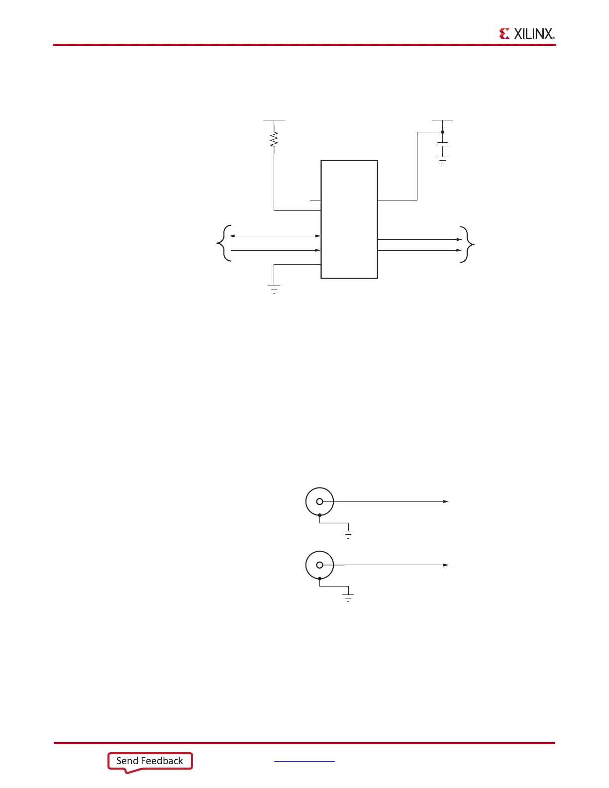
For more details, see the Silicon Labs Si570 data sheet [Ref 19]. The user clock circuit is
shown in Figure 1-10.
Note:
In Figure 1-10, USER_CLOCK_N and USER_CLOCK_P are differential clock signals.
User SMA Clock (USER_SMA_CLOCK_P and USER_SMA_CLOCK_N)
[Figure 1-2, callout 9]
An external high-precision clock signal can be provided to the FPGA bank 14 by
connecting differential clock signals through the onboard 50Ω SMA connectors J31 (P) and
J32 (N). The differential clock signal names are USER_SMA_CLOCK_P and
USER_SMA_CLOCK_N, which are connected to FPGA U1 pins AJ32 and AK32
respectively. The user-provided 1.8 V differential clock circuit is shown in Figure 1-11.
X-Ref Target - Figure 1-10
Figure 1-10: User Clock Source
UG885_c1_10_021412
GND
VCC3V3
Si570
Programmable
Oscillator
NC
OE
GND
SCL
SDA
VDD
1
2
3
8
7
6
U34
R15
4.7KΩ 5%
USER CLOCK N
C192
0.01 μF 25V
X7R
CLK-
4
5
GND
VCC3V3
CLK+
USER CLOCK P
USER CLOCK SDA
USER CLOCK SCL
10 MHz - 810 MHz
50 PPM
To
I
2
C
Bus Switch
(U52)
X-Ref Target - Figure 1-11
Figure 1-11: User SMA Clock Source
USER_SMA_CLOCK_P
J32
USER_SMA_CLOCK_N
GND
J31
GND
UG885_c1_11_020612
SMA
Connector
SMA
Connector

 Loading...


