EasyManua.ls Logo

Xilinx Virtex-5 RocketIO GTP User Manual

Xilinx Virtex-5 RocketIO GTP
316 pages
To Next Page IconTo Next Page
To Previous Page IconTo Previous Page
Page #61 background imageLoading...
Page #61 background image
Virtex-5 RocketIO GTP Transceiver User Guide www.xilinx.com 61
UG196 (v1.3) May 25, 2007
Shared PMA PLL
R
Table 5-2 defines the shared PMA PLL attributes.
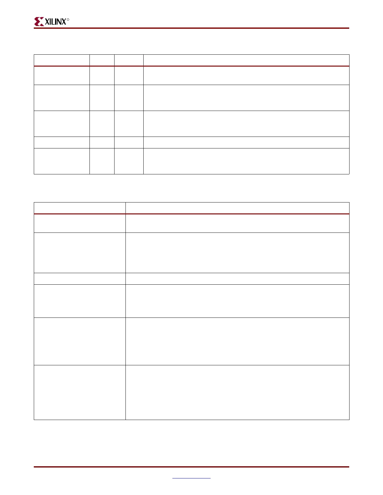
Table 5-1: Shared PMA PLL Ports
Port Dir Domain Description
CLKIN In Async
Reference clock input to the shared PMA PLL. See “Clocking,” page 68 for
more information about the different ways this port can be driven.
INTDATAWIDTH In Async
Sets the internal datapath width for the GTP_DUAL. If set to 0, the internal
datapath width is set to 8 bits. If set to 1, the internal datapath width is set to
10 bits.
PLLLKDET Out Async
This port indicates that the VCO rate is within acceptable tolerances of the
desired rate when High. Neither GTP transceiver in the tile operates reliably
until this condition is met.
PLLLKDETEN In Async This port enables the PLL lock detector and should always be tied High.
REFCLKOUT Out Async
The REFCLKOUT port from each GTP_DUAL tile provides direct access to
the reference clock provided to the shared PLL (CLKIN). It can be routed for
use in the FPGA logic.
Table 5-2: Shared PMA PLL Attributes
Attribute Description
PCS_COM_CFG[27:0]
(1
For PLL_DIVSEL_FB = 1, set PCS_COM_CFG to 28’h1680A07, otherwise set to
28’h1680A0E (default).
PLL_DIVSEL_FB
Controls the feedback divider. Valid settings for PLL_DIVSEL_FB are 1, 2, 3, 4, and 5.
PLL_DIVSEL_FB is multiplied by 4 or 5, depending on the width of the internal
datapath as set by INTDATAWIDTH. If INTDATAWIDTH is Low, the feedback
divider N is set to PLL_DIVSEL_FB x 4. If INTDATAWIDTH is High, the feedback
divider N is set to PLL_DIVSEL_FB x 5.
PLL_DIVSEL_REF Controls the reference clock divider. Valid settings for PLL_DIVSEL_REF are 1 and 2.
PLL_RXDIVSEL_OUT_0
PLL_RXDIVSEL_OUT_1
Divides the PLL clock to produce a high-speed RX clock. Because both edges of the
clock are used, the divided clock must run at 1/2 the desired RX line rate. Permitted
divider settings are 1, 2, and 4. See “Serial In to Parallel Out (SIPO),” page 141 for
details.
PLL_TXDIVSEL_COMM_OUT
Divides the PLL clock to produce a high-speed TX clock. Because both edges of the
clock are used, the divided clock must run at 1/2 the desired TX line rate. Permitted
divider settings are 1, 2, and 4. This divider provides a clock to both GTP transceivers
and should be used when the same divider value is needed for both. When
PLL_TXDIVSEL_COMM_OUT is used, both PLL_TXDIVSEL_OUT attributes must
be set to 1. See “Parallel In to Serial Out (PISO),” page 110 for details.
PLL_TXDIVSEL_OUT_0
PLL_TXDIVSEL_OUT_1
Divides the PLL clock to produce a high-speed TX clock. Because both edges of the
clock are used, the divided clock must run at 1/2 the desired TX line rate. Permitted
divider settings are 1, 2, and 4. Each GTP transceiver has its own
PLL_TXDIVSEL_OUT. If the transceivers require different dividers, these attributes
must be used instead of PLL_TXDIVSEL_COMM_OUT, and
PLL_TXDIVSEL_COMM_OUT must be set to 1. See “Parallel In to Serial Out
(PISO),” page 110 for details.
Notes:
1. In ISE 9.2i and above, this attribute is included in the GTP_DUAL instance. Older ISE versions require setting this attribute with the
a user-constraints file (UCF) when a non-default value is needed.

Table of Contents

Question and Answer IconNeed help?

Do you have a question about the Xilinx Virtex-5 RocketIO GTP and is the answer not in the manual?

Xilinx Virtex-5 RocketIO GTP Specifications

General IconGeneral
BrandXilinx
ModelVirtex-5 RocketIO GTP
CategoryTransceiver
LanguageEnglish

Summary

Revision History

About This Document

Section 1: FPGA Level Design

Chapter 1: Introduction to the RocketIO GTP Transceiver

GTP Transceiver Overview

Introduces the Virtex-5 RocketIO GTP transceiver and its features.

Chapter 2: RocketIO GTP Transceiver Wizard

GTP Transceiver Wizard Usage

Details on using the RocketIO GTP Transceiver Wizard for wrapper generation.

Chapter 3: Simulation

Simulation Overview

Covers prerequisites and environment setup for simulating GTP transceiver designs.

Simulation Ports and Attributes

Details simulation-only ports and attributes for the GTP_DUAL tile.

Simulation SmartModel Attributes

Explains attributes controlling SmartModel behavior for simulation accuracy.

Chapter 4: Implementation

Implementation Overview

Provides information on mapping GTP_DUAL tiles to device resources and package combinations.

Implementation Description

Explains GTP_DUAL tile positioning and UCF creation methods.

GTP_DUAL Package Placement

Illustrates GTP_DUAL placement for various packages and nomenclature.

Chapter 5: Tile Features

GTP Tile Features Overview

Overview of shared GTP functions for power, clocking, resets, and reconfiguration.

Shared PMA PLL Overview

Describes the shared PMA PLL used for generating high-speed serial clocks.

GTP Clocking Overview

Explains methods for driving the CLKIN port for GTP transceivers.

GTP Reset Overview

Details the three ways to reset a GTP_DUAL tile and its subcomponents.

GTP Power Control Overview

Discusses power control modes for generic and protocol-specific power management.

DRP Overview

Explains the DRP interface for dynamic parameter changes of the GTP_DUAL tile.

Chapter 6: GTP Transmitter (TX)

GTP Transmitter Overview

Overview of the GTP transmitter, including PCS and PMA blocks.

FPGA TX Interface Details

Describes the interface for transmitting parallel data to the GTP transceiver.

8B/10B Encoder Functionality

Details the 8B/10B encoder for outgoing data, its benefits, and costs.

TX Buffering and Phase Alignment Overview

Explains TX buffer, phase alignment, and bypass options to resolve clock domain differences.

Chapter 7: GTP Receiver (RX)

GTP Receiver Overview

Overview of the GTP receiver, including PCS and PMA blocks.

RX Termination and Equalization Details

Details circuits for optimizing termination and compensating for high-frequency losses.

RX Clock Data Recovery Details

Describes the CDR circuit's function in recovering the clock from incoming serial data.

Comma Alignment and Detection Details

Details the alignment block for aligning specific commas to byte boundaries.

Chapter 8: Cyclic Redundancy Check (CRC)

CRC Block Overview

Shows the basic port interface and operation of the CRC block.

CRC for Error Checking

Explains how CRC is used as an error-checking mechanism for data frames.

CRC Primitive Details

Describes the CRC32 and CRC64 primitives used for CRC calculation.

Chapter 9: Loopback

Loopback Modes Explained

Explains loopback modes and their categories: near-end and far-end.

Loopback Configuration Ports and Attributes

Defines the ports and attributes for configuring loopback modes.

Near-End PMA Loopback Mode

Details Near-End PMA loopback mode using the Near-End source for data generation.

Chapter 10: GTP-to-Board Interface

Analog Design Guidelines for GTP

Discusses power supply and clocking design guidelines for overall system performance.

REFCLK Selection Guidelines

Focuses on selecting the reference clock source or oscillator based on characteristics.

SelectIO Crosstalk Guidelines for GTP

Provides guidelines for SelectIO usage to minimize impact on GTP transceiver performance.

Chapter 11: Design Constraints Overview

Physical Interconnect Topology Overview

Defines a physical link between transceivers as a channel.

PCB Materials and Traces Overview

Discusses PCB materials and trace design for optimal performance.

Powering Transceivers Overview

Discusses power supply designs for transceivers to achieve low link error rates.

Chapter 12: PCB Materials and Traces

Dielectric Losses

Discusses signal energy loss due to dielectric characteristics.

Choosing the Substrate Material

Provides guidance on selecting substrate materials for performance and cost.

Trace Routing

Provides guidelines for routing high-speed differential traces.

Chapter 13: Design of Transitions

Excess Capacitance and Inductance

Discusses excess capacitance and inductance in differential transitions.

Time Domain Reflectometry (TDR)

Explains TDR techniques for identifying transition issues.

Differential Vias

Explains the common transition type for differential signals using GSSG vias.

Chapter 14: Guidelines and Examples

Summary of Guidelines

Provides a quick reference to guidelines and strategies for high-speed serial channels.

BGA Escape Example

Illustrates routing transceiver signal pairs along BGA edges.

Section 3: Appendices

MGT to GTP Transceiver Design Migration

Describes differences migrating from Virtex-II Pro/Virtex-4 MGTs to Virtex-5 GTP transceivers.

OOB/Beacon Signaling

Provides support for Out-of-Band (OOB) signaling for SATA and beaconing.

8B/10B Valid Characters

Lists valid Data characters and K characters for 8B/10B encoding.

DRP Address Map of the GTP_DUAL Tile

Lists attributes and their mappings to DRP addresses and bit locations.

Low Latency Design

Illustrates the latency of functional blocks within the Transmit and Receive sections.

Related product manuals