ZCU111 Board User Guide 55
UG1271 (v1.1) August 6, 2018 www.xilinx.com
Chapter 3: Board Component Descriptions
Tab l e 3- 1 8 and Table 3 -19 provides guidance on external clocking modifications.
IMPORTANT: To provide external sources from the RFMC connector, the default capacitors must be
carefully moved to optional capacitor locations.
By default, the LMK04208 provides a clock to the DAC bank 228 SYSREF clock input pins.
IMPORTANT: To provide an external SYSREF clock with the onboard optional SMAs, the default
capacitors must be carefully moved to optional capacitor locations.
Before making ZCU111 RF clock capacitor modifications, refer to the PC board layout and
identify the metal RF cage associated with the capacitors of interest:
• C632/C640, C646/C718: RFCAGE2
• C683/C690, C692/C699: REFCAGE3
• C666/C673, C675/C682: RFCAGE4
• C742 and C743: RFCAGE1
The appropriate cage lid must be removed to make the capacitor modifications, and
replaced upon completion.
To implement the external clock source capability, remove (desolder) the default capacitors
and solder them onto the pads at the optional external source capacitors locations shown in
the above tables (e.g., for Tabl e 3-1 8, U102 Channel A, remove C632 and solder it at C948,
remove C640 and solder it at C949, and so on). Due to via-in-pad component footprints,
Xilinx recommends the rework be implemented by an expert rework technician.
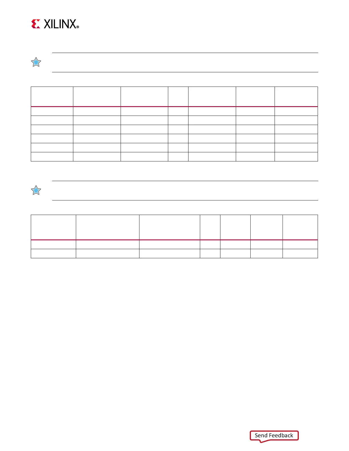
Table 3-18: RFMC External Clocking Modifications
LMX2594 Device
and Channel
Output Net Name FPGA Net Name
FPGA
Bank
RFMC Optional
External Clock
Net Name
Default
Capacitors
Optional External
Source Capacitors
U102 Channel A RF1_CLKO_A_P/N RF1_CLKO_A_C_P/N 224 ADCLK_IN0_P/N C632 / C640 C948 / C949
U102 Channel B RF1_CLKO_B_P/N RF1_CLKO_B_C_P/N 225 ADCLK_IN1_P/N C646 / C718 C1018 / C1019
U103 Channel A RF2_CLKO_A_P/N RF2_CLKO_A_C_P/N 227 ADCLK_IN2_P/N C683 / C690 C951 / C950
U103 Channel B RF2_CLKO_B_P/N RF2_CLKO_B_C_P/N 226 ADCLK_IN3_P/N C692 / C699 C1020 / C1021
U104 Channel A RF3_CLKO_A_P/N RF3_CLKO_A_C_P/N 228 DACLK_IN0_P/N C666 / C673 C1024 / C1025
U104 Channel B RF3_CLKO_B_P/N RF3_CLKO_B_C_P/N 229 DACLK_IN1_P/N C675 / C682 C1022 / C1023
Table 3-19: SYSREF External Clocking Modifications
LMK04208 Device
and Channel
Output Net Name FPGA Net Name
FPGA
Bank
ZCU111
SYSREF SMA
Default
Capacitors
Optional
External
Source
Capacitors
U90 OUT1 P CLK_4208_OUT1_P SYSREF_RFSOC_C_P 228 J7 C742 C1031
U90 OUT1 N CLK_4208_OUT1_N SYSREF_RFSOC_C_N 228 J10 C743 C1034

 Loading...


