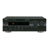
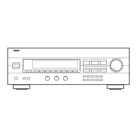
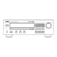
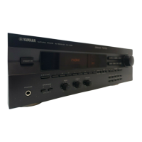
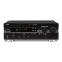
101
RX-V3900/DSP-AX3900
RX-V3900/
DSP-AX3900
IC114: MB87L8760 (D-VIDEOP.C.B)
NPGA
* No replacement part available. /
サービス部品供給なし
Pin No. Port Name Function Name (P.C.B.) I/O Detail of Function
1 VDD MCU
2 VSS MCU
3 PIO[0] VDEC_N_INT IRQ Interrupt from ADV7800
4 PIO[1] HTX1_N_INT IRQ Interrupt from SII9134 #1
5 PIO[2] HTX2_N_INT IRQ Interrupt from SII9134 #2
6 PIO[3] HRX_N_INT IRQ Interrupt from SII9135A
7 PIO[4] HEQ0_N_INT_F IRQ Interrupt from SII9185A #0
8 PWM[0] –
9 VSS MCU
10 VDD MCU
11 SCL0 HEQ_SCL SO SII9185A control
12 SDA0 HEQ_SDA SIO SII9185A control
13 PIO[16] IOEX_N_CS O I/O expanded device chip select
14 PIO[17] VIPC_N_CS O
15 PIO[18] CXB1442_CE O CXB1442 chip enable
16 PIO[19] FPGA_N_CS O FPGA chip select
17 PIO[20] FPGA_N_CFG O FPGA configuration
18 VDD MCU
19 VSS MCU
20 PIO[21] FPGA_CDONE I FPGA configuration
21 PIO[22] FPGA_N_STA I FPGA configuration
22 PIO[23] HDMI_MUT_3 I HDMI Mute input
23 PWM[1] –
24 PIO[5] HEQ1_N_INT_F IRQ Interrupt from SII9185A #1
25 SCL1 DV_SCL SO
Video Encoder/Decoder ABT2010 analog video
device control
26 SDA1 DV_SDA SIO
Video Encoder/Decoder ABT2010 analog video
device control
27 SCL2 EEP_SCL SO EEPROM
read/write
28 SDA2 EEP_SDL SIO EEPROM
read/write
29 VDD MCU
30 VSS MCU
31 PIO[6] PHY_N_INT IRQ Interrupt from PHY
32 SCK0 FPGA_SCK SO FGPA control
33 SO0 FPGA_MOSI SO FGPA control
34 SI0 FPGA_MISO SI FGPA control
35 PIO[7] –
36 PIO[8] HTX1_N_RST O SII9134 #1 reset
37 VDD MCU
38 VSS MCU
39 PIO[24] HTX_AUSEL O
Source selector when updating HDMI conversion
L: HDMI input / H: Analog input
40 SCK1 IOEX_N_SCK SO Serial clock for I/O expanded device chip
41 SO1 IOEX_MOSI SO Serial data for I/O expanded device chip
42 SI1 –
43 SCK2 VIPC_N_SCK
44 SO2 VIPC_MOSI
45 VSS MCU
46 VDD MCU
47 SI2 VIPC_MISO
48 TXD0 –
49 RXD0 –
50 PI4_XCTS0 –
51 PO4_XRTS0 –
52 PIO[25] VDEC_FPGA_N_OE O
Path from ADV7800 to FPGA ON/OFF
(L: ON / H: OFF)
53 PIO[26] LPF_HD O
LPF switching
L: when SD, PS signal is input
H: when HD signal is input
 Loading...