CB401
IC402
IC401
CB402
CB416
CB403
CB404
CB405
CB406
CB407
CB409
CB410
CB411
IC407
IC403
IC406
CB413
CB414
CB412
JK401
JK402
JK403
JK404
A
1
2
3
4
5
6
7
8
9
10
BCDEFGH I J K
L MN
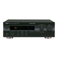
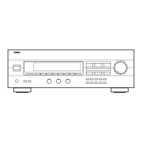
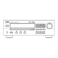
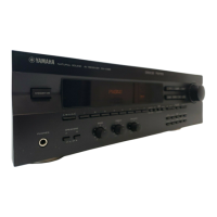
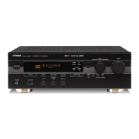
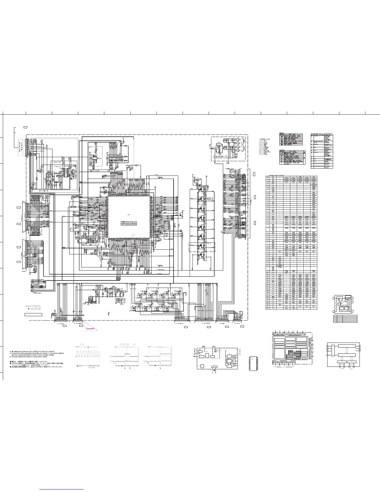
RX-V3900/DSP-AX3900
148
FUNCTION 1/4
0
0
0
5.2
5.1
5.0 5.1
00
0
0
0
0
5.0
5.1
0
0
5.0
0
5.0
5.0
0
0
5.0
0
0
0
5.0
5.4
5.0
5.0
5.1
2.4
5.0
2.5
4.9
0
5.0
0
5.0
5.0
0
0
0
5.1
5.0
0
5.0
5.0
5.1
5.2
0
5.0
5.0
0
12.4
5.0
4.9
0
5.2
5.1
5.0
0
0
4.3
0
13.2
4.9
0
5.4
5.8
4.9
11.9
11.9
-11.8
-11.8
11.9
11.9
-11.8
-11.8
-11.7
0
0
1.1
4.6
-12.0
-11.8
0.4
0
0
0
0
1.1
5.2
1.1
1.1
5.0
5.0
3.2
5.2
2.3
3.7
0
5.0
0
5.0
0
0
0
0
0
0
0
0
0
0
0
0
13.2
13.2
0
5.8
5.8
5.1
5.2
0
0
5.0
5.2
5.1
0
0
12.0
-11.8
0
0
0
12.0
-11.8
-11.8
5.1
0
0
12.0
11.9
0
0
0
12.0
5.1
0
0
12.0
11.9
5.1
0
0
12.0
11.9
11.9
0
0
0
12.0
-11.8
5.1
0
0
12.0
3.7
5.0
0
0
0
0
5.0
5.0
0
0
5.0
5.0
0
5.1
0
5.0
5.0
5.0
4.8
0
0
4.9
4.9
5.0
5.0
0
0
5.0
0
4.8 0
5.2 5.1
5.0 5.1
00
5.2
4.8
5.1
00
0
3.7
0
0
0
0
0
0
0
0
0
5.1
5.1
0
0
0
0
0
0
0
0
0
5.1
5.1
4.9
0
5.0
0
0
0
0
5.2
5.0
5.0
5.2
5.2
5.0
0
5.0
0
5.0
0
0
0
0
5.0
0
0
5.0
0
5.2
5.2
5.1
5.2
0
5.0
5.0
0
0
0
0
0
5.2
4.8
13.2
-12.0
5.0
5.0
0
5.0
5.0
12.4
5.0
5.0
4.9
5.0
12.0
0
5.0
4.9
0
5.0
-12.0
5.0
5.0
-12.0
0
5.0
-12.0
0
5.0
5.0
0
5.0
0
0
5.0
-12.0
5.0
5.1
0
0
0
5.0
5.0
0
5.0
5.2
5.2
5.2
0
5.0
5.0
1.1
2.3
5.0
0
4.3
0
1.1
1.1
0.4
1.1
0
5.2
1.1
0
0
5.2
5.0
0.4
0
5.2
5.2
1.1
5.0
5.1
5.0
1.1
0
5.0
5.1
4.6
0.4
0
0
5.0
0
0
5.0
5.2
5.0
0
5.0
0
0
0
0
5.0
5.0
0
0
0
0
5.0
5.0
5.0
0
5.0
5.0
0
5.1
5.0
0
5.0
5.0
0
5.0
5.0
0
5.0
0
0
0
5.0
5.0
5.0
0
0
5.0
5.0
0
5.0
5.0
5.0
5.0
0
0
0
0
5.0
5.0
0
0
5.0
5.0
4.9
4.9
5.0
5.0
6.4
-6.3
-12.0
-12.0
-12.0
5.0
0
0
5.0
0
0
0
12.0
-12.0
12.0
5.0
0
0
5.0
A-1
A-2
1
A-3
2
FUNCTION (1)
to FUNCTION 2/4
(B, G, E models)
(U, C, R, T, K, A, B, G, E, L models)
(U, C, R, T, K, A, B, G, E, L models)
MICROPROCESSOR
Serial/Parallel (Port Extend)
(MAIN)
REMOTE
to FUNCTION 2/4
IC403: LC709004A-TLM-E
I/O-expander for microcontroller
Control logic
port 0 I/O buffer
Serial/parallel converter/shift register
I/O control/output register
DIN
VDD
DOUT
VSS
CLK#
CS#
RES#
P00
P07
2
14
15
19
3
4
21
24 17
port 1 I/O buffer
P10
P17
15 8
POINT A-1 XL402 (Pin 20 of IC402)
POINT A-2 A-3 1 / Pin7, 2 / Pin8 of CB406
1+5V
/RES
2
1+5V
/RES
2
AC cable ON AC cable OFF AC cable ON
VDD
CE
3
1
5
2
V
OUT
4
NC
GND
Vref
Short
Protection
Circuit
Current
Limit
Circuit
Thermal
Protection
IC407: R1154H058B-T1-F
Voltage regulator
Pin No.
1
2
3
4
5
Symbol
V
OUT
GND
CE
NC†
V
DD
Description
Output Pin for Voltage Regulator
Ground
Chip Enable Pin (active at "H")
No Connection
Power Supply Pin
REFERENCE
VOLTAGE
CINFLOUTVREF
VREF
ANTIALIASING
FILTER
57kHz
BPF
(SCF)
SMOOTHING
FILTER
MPXIN
+3V
Vdda
Vssa
PLL
(57kHz)
CLOCK
RECOVERY
(1187.5Hz)
+3V
Vddd
RDS-ID/
READY
RST
Vssd
DATA
DECODER
XOUTXIN
TEST
TEST
CLK(4.332MHz)
OSC
RAM
(128bits)
RDDA
RDCL
RDS-ID
DETECT
MODE
IC401: LC72725KM-UY-TLM-E
RDS signal demodulation IC
CIN
TEST
Vssd
MODE
Vddd
XIN
XOUT
RST
RDCL
FLOUT
RDS-ID/READY
RDDA
VREF
MPXIN
Vdda
Vssa
2
3
4
5
6
7
8
9
10
11
12
13
14
15
16
1
IC402: M3087BFKBGP
Microprocessor
Port P0 Port P1 Port P2 Port P3 Port P4 Port P5 Port P6
Port P7
Port P14 Port P15 Port P11 Port P12
Port P10Port P9Port P8
P85
Port P13
R0H R0L
R1H R1L
R2
R3
A0
A1
FB
SB
NOTES:
1. Ports P11 to P15 are provided in the 144-pin package only.
2. Included in the 144-pin package only.
3.The supply voltage of M32C/84T (High-reliability version) must be V
CC1=VCC2.
FLG
INTB
ISP
USP
PC
SVF
SVP
VCT
Multiplier
M32C/80 series microproce ssor core
Clock Generation Circuit
XIN - XOUT
XCIN - XCOUT
On-chip Oscillator
PLL Frequency Synthesizer
A/D Converter:
1 circuit
Standard: 10 inputs
Maximum: 34 inputs
(2)
UART/Clock Synchronous Serial I/O:
5-channel
CRC Calculation Circuit (CCITT):
X
16
+X
12
+X
5
+1
X/Y Converter:
16-bit x 16-bit
D/A Converter:
8-bit x 2-channel
Peripheral Functions
<VCC2
(3)
>
<
VCC1
(3)
>
<VCC1
(3)
>
ROM
RAM
Memory
<VCC1
(3)
>
<VCC2
(3)
>
78 58 8
(Note 1)
8
8
7
888888 8
8
DMACII
DMAC
Watchdog Timer (15-bit)
CAN Module: 1-channel
Intelligent I/O
Time Measurement: 8-channel
Waveform Generating: 8-channel
Communication Functions:
Clock Synchronous Serial I/O, UART,
HDLC Data Processing
Timer (16-bit)
Timer A: 5-channel
Timer B: 6-channel
Three-Phase Motor Control Circuit
to FL (5)_CB960
Page 168
M6
to FL (5)_CB972
Page 168
L6
to FL (3)_CB955
Page 168
N8
to FL (3)_CB952
Page 168
M8
to FL (2)_CB962
Page 168
G7
to FL (2)_CB969
Page 168 H7
to FL (2)_CB958
Page 168
E7
to FL (6)_W9901
Page 167
N3
to CONNECT (1)_CB903 (U model)
Page 169
B7
to POWER (4)_W1
Page 154
J8
to MAIN (4)_W272
Page 153
B1
to POWER (3)_CB18
Page 154
H7
to A-VIDEO_CB203
Page 156
J2
to DSP_CB504
Page 145
F1
To AM/FM TUNER (C, R, T, K, A, B, G, E, L, J models)
(C, R, T, K, A, B, G, E, L, J models)
 Loading...