LMK04821
,
LMK04826
,
LMK04828
SNAS605AR –MARCH 2013–REVISED DECEMBER 2015
www.ti.com
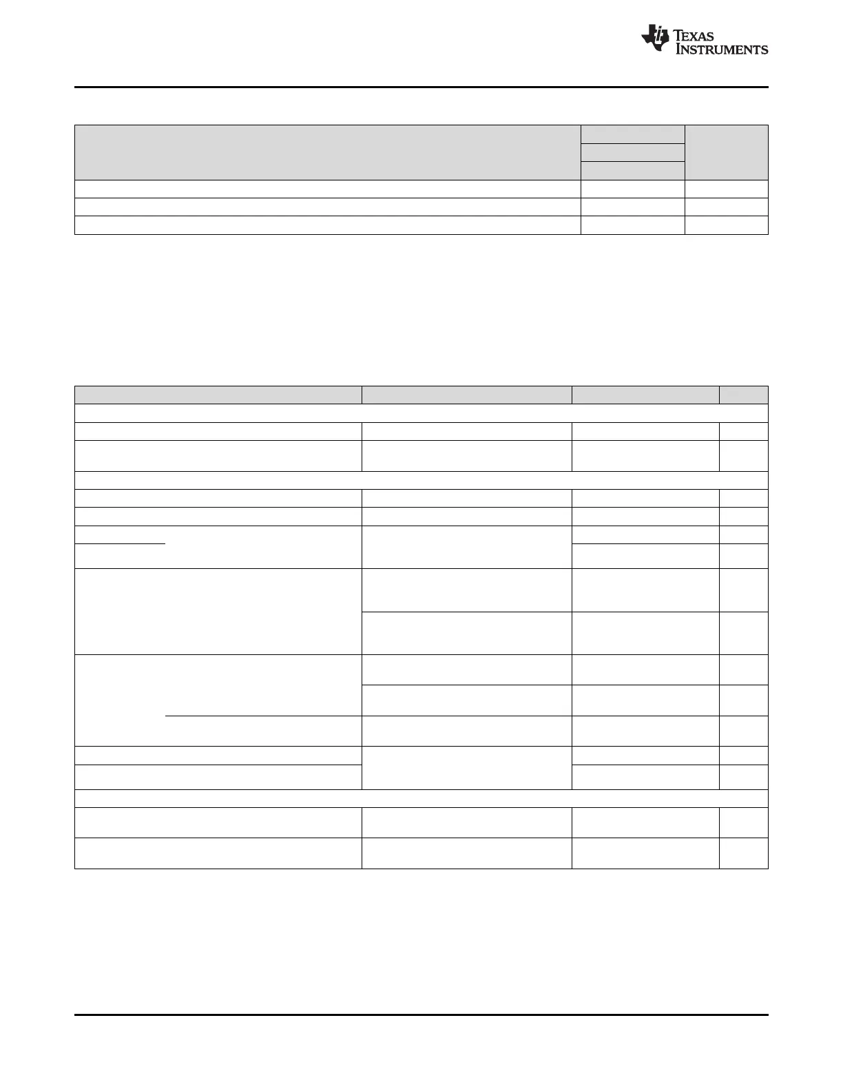
Thermal Information (continued)
LMK0482x
THERMAL METRIC
(1)
NKD (WQFN) UNIT
64 PINS
ψ
JT
Junction-to-top characterization parameter
(5)
0.1 °C/W
ψ
JB
Junction-to-board characterization parameter
(6)
3.5 °C/W
R
θJC(bot)
Junction-to-case (bottom) thermal resistance
(7)
0.7 °C/W
(5) The junction-to-top characterization parameter, Ψ
JT
, estimates the junction temperature of a device in a real system and is extracted
from the simulation data for obtaining R
θJA
, using a procedure described in JESD51-2a (sections 6 and 7).
(6) The junction-to-board characterization parameter, Ψ
JB
estimates the junction temperature of a device in a real system and is extracted
from the simulation data for obtaining R
θJA
, using a procedure described in JESD51-2a (sections 6 and 7).
(7) The junction-to-case(bottom) thermal resistance is obtained by simulating a cold plate test on the exposed (power) pad. No specific
JEDEC standard test exists, but a close description can be found in the ANSI SEMI standard G30-88.
7.5 Electrical Characteristics
(3.15 V < V
CC
< 3.45 V, –40 °C < T
A
< 85 °C and T
PCB
≤ 105 °C. Typical values at V
CC
= 3.3 V, T
A
= 25 °C, at the
Recommended Operating Conditions and are not assured.)
PARAMETER TEST CONDITIONS MIN TYP MAX UNIT
CURRENT CONSUMPTION
I
CC_PD
Power Down Supply Current 1 3 mA
14 HSDS 8 mA clocks enabled
I
CC_CLKS
Supply Current
(1)
565 665 mA
PLL1 and PLL2 locked.
CLKin0/0*, CLKin1/1*, and CLKin2/2* INPUT CLOCK SPECIFICATIONS
f
CLKin
Clock Input Frequency 0.001 750 MHz
SLEW
CLKin
Clock Input Slew Rate
(2)
20% to 80% 0.15 0.5 V/ns
V
ID
CLKin Clock Input 0.125 1.55 |V|
Differential Input Voltage
(3)
AC coupled
V
SS
CLKin 0.25 3.1 Vpp
Figure 8
AC coupled to CLKinX;
CLKinX* AC coupled to Ground 0.25 2.4 Vpp
CLKinX_TYPE = 0 (Bipolar)
Clock Input
V
CLKin
Single-ended Input Voltage
AC coupled to CLKinX;
CLKinX* AC coupled to Ground 0.35 2.4 Vpp
CLKinX_TYPE = 1 (MOS)
Each pin AC coupled, CLKin0/1/2
0 |mV|
CLKinX_TYPE = 0 (Bipolar)
DC offset voltage between
CLKinX/CLKinX* (CLKinX* - CLKinX)
Each pin AC coupled, CLKin0/1
|V
CLKinX-offset
| 55 |mV|
CLKinX_TYPE = 1 (MOS)
DC offset voltage between Each pin AC coupled
20 |mV|
CLKin2/CLKin2* (CLKin2* - CLKin2) CLKinX_TYPE = 1 (MOS)
V
CLKin-
V
IH
High input voltage DC coupled to CLKinX; 2.0 V
CC
V
CLKinX* AC coupled to Ground
V
CLKin-
V
IL
Low input voltage 0.0 0.4 V
CLKinX_TYPE = 1 (MOS)
FBCLKin/FBCLKin* and Fin/Fin* INPUT SPECIFICATIONS
Clock Input Frequency for AC coupled
f
FBCLKin
0.001 750 MHz
0-delay with external feedback. CLKinX_TYPE = 0 (Bipolar)
Clock Input Frequency for AC coupled
(4)
f
Fin
0.001 3100 MHz
external VCO or distribution mode. CLKinX_TYPE = 0 (Bipolar)
(1) See the applications section of Power Supply Recommendations for Icc for specific part configuration and how to calculate Icc for a
specific design.
(2) In order to meet the jitter performance listed in the subsequent sections of this data sheet, the minimum recommended slew rate for all
input clocks is 0.5 V/ns. This is especially true for single-ended clocks. Phase noise performance will begin to degrade as the clock input
slew rate is reduced. However, the device will function at slew rates down to the minimum listed. When compared to single-ended
clocks, differential clocks (LVDS, LVPECL) will be less susceptible to degradation in phase noise performance at lower slew rates due to
their common mode noise rejection. However, it is also recommended to use the highest possible slew rate for differential clocks to
achieve optimal phase noise performance at the device outputs.
(3) See Differential Voltage Measurement Terminology for definition of V
ID
and V
OD
voltages.
(4) Assured by characterization. ATE tested at 2949.12 MHz.
10 Submit Documentation Feedback Copyright © 2013–2015, Texas Instruments Incorporated
Product Folder Links: LMK04821 LMK04826 LMK04828
 Loading...


