SDCLKout1
SCK
SDIO
CS*
NC
NC
NC
Vcc1_VCO
LDObyp1
LDObyp2
Status_LD1
Vcc9_CP2
Vcc7_OSCout
Vcc12_CG0
CPout2
Vcc10_PLL2
DCLKout4*
DCLKout4
OSCin
OSCin*
CPout1
Vcc8_OSCin
CLKin0
CLKin0*
SDCLKout3*
SDCLKout3
Vcc2_CG1
DCLKout2
DCLKout2*
1
2
3
4
5
6
7
8
9
10
11
12
13
14
15
16
32
31
30
29
28
27
26
25
24
23
22
21
20
19
18
17
48
47
46
45
44
43
42
41
40
39
38
37
36
35
34
33
49
50
51
52
53
54
55
56
57
58
59
60
61
62
63
64
SDCLKout1*
Vcc11_CG3
DCLKout10
SYNC/SYSREF_REQ
Vcc6_PLL1
CLKin1/Fin/FBCLKin
CLKin1*/Fin*/FBCLKin*
CLKin_SEL1
DCLKout0
DCLKout0*
SDCLKout11*
DCLKout10*
SDCLKout11
SDCLKout5
SDCLKout5*
OSCout*/CLKin2*
OSCout/CLKin2
SDCLKout13
DCLKout12*
SDCLKout13*
DCLKout12
SDCLKout7*
SDCLKout7
DCLKout6*
DCLKout6
SDCLKout9
DCLKout8*
SDCLKout9*
DCLKout8
Vcc4_CG2
Status_LD2
RESET/GPO
CLKin_SEL0
Vcc3_SYSREF
LLP-64
Top down view
DAP
Vcc5_DIG
Clock Group 1
Clock Group 0
Clock Group 2
Clock Group 3
LMK04821
,
LMK04826
,
LMK04828
www.ti.com
SNAS605AR –MARCH 2013–REVISED DECEMBER 2015
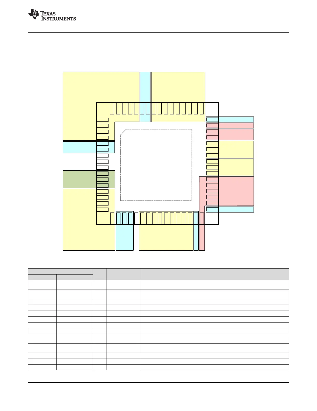
6 Pin Configuration and Functions
NKD Package
64-Pin WQFN
Top View
Pin Functions
PIN
I/O TYPE DESCRIPTION
(1)
NO. NAME
DCLKout0,
1, 2 O Programmable Device clock output 0.
DCLKout0*
SDCLKout1,
3, 4 O Programmable SYSREF / Device clock output 1
SDCLKout1*
5 RESET/GPO I CMOS Device reset input or GPO
6 SYNC/SYSREF_REQ I CMOS Synchronization input or SYSREF_REQ for requesting continuous SYSREF.
7, 8, 9 NC Do not connect. These pins must be left floating.
10 Vcc1_VCO PWR Power supply for VCO LDO.
11 LDObyp1 ANLG LDO Bypass, bypassed to ground with 10-µF capacitor.
12 LDObyp2 ANLG LDO Bypass, bypassed to ground with a 0.1-µF capacitor.
SDCLKout3,
13, 14 O Programmable SYSREF / Device Clock output 3.
SDCLKout3*
DCLKout2,
15, 16 O Programmable Device clock output 2.
DCLKout2*
17 Vcc2_CG1 PWR Power supply for clock outputs 2 and 3.
18 CS* I CMOS Chip Select
19 SCK I CMOS SPI Clock
(1) See Pin Connection Recommendations for recommended connections.
Copyright © 2013–2015, Texas Instruments Incorporated Submit Documentation Feedback 7
Product Folder Links: LMK04821 LMK04826 LMK04828
 Loading...


