LMK04821
,
LMK04826
,
LMK04828
www.ti.com
SNAS605AR –MARCH 2013–REVISED DECEMBER 2015
9.7.3.10 SYSREF_CLR, SYNC_1SHOT_EN, SYNC_POL, SYNC_EN, SYNC_PLL2_DLD, SYNC_PLL1_DLD,
SYNC_MODE
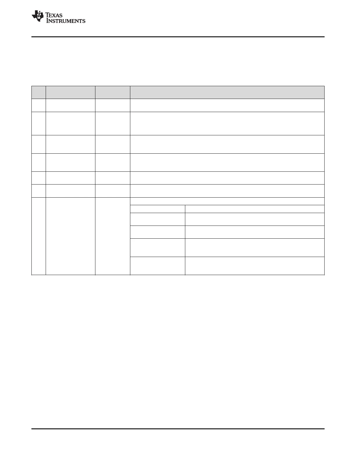
This register sets general SYNC parameters such as polarization, and mode. Refer to Figure 13 for block
diagram. Refer to Table 1 for using SYNC_MODE for specific SYNC use cases.
Table 32. Register 0x143
POR
BIT NAME DESCRIPTION
DEFAULT
Except during SYSREF Setup Procedure (see SYNC/SYSREF), this bit should always be
7 SYSREF_CLR 1
programmed to 0. While this bit is set, extra current is used. Refer to Table 84.
SYNC one shot enables edge sensitive SYNC.
0: SYNC is level sensitive and outputs will be held in SYNC as long as SYNC is asserted.
6 SYNC_1SHOT_EN 0
1: SYNC is edge sensitive, outputs will be SYNCed on rising edge of SYNC. This results in
the clock being held in SYNC for a minimum amount of time.
Sets the polarity of the SYNC pin.
5 SYNC_POL 0 0: Normal
1: Inverted
Enables the SYNC functionality.
4 SYNC_EN 1 0: Disabled
1: Enabled
0: Off
3 SYNC_PLL2_DLD 0
1: Assert SYNC until PLL2 DLD = 1
0: Off
2 SYNC_PLL1_DLD 0
1: Assert SYNC until PLL1 DLD = 1
Sets the method of generating a SYNC event.
Field Value SYNC Generation
Prevent SYNC Pin, SYNC_PLL1_DLD flag, or SYNC_PLL2_DLD
0 (0x00)
flag from generating a SYNC event.
SYNC event generated from SYNC pin or if enabled the
1 (0x01)
SYNC_PLL1_DLD flag or SYNC_PLL2_DLD flag.
1:0 SYNC_MODE 1
For use with pulser - SYNC/SYSREF pulses are generated by
2 (0x02) pulser block via SYNC Pin or if enabled SYNC_PLL1_DLD flag
or SYNC_PLL2_DLD flag.
For use with pulser - SYNC/SYSREF pulses are generated by
3 (0x03) pulser block when programming register 0x13E
(SYSREF_PULSE_CNT) is written to (see ).
Copyright © 2013–2015, Texas Instruments Incorporated Submit Documentation Feedback 67
Product Folder Links: LMK04821 LMK04826 LMK04828
 Loading...


