DCLKout0
368.64 MHz
DCLKout2
368.64 MHz
First
Adjustment
VCO
2949.12 MHz
DCLKout2
368.64 MHz
Second
Adjustment
CNTH = 4 CNTL = 5
CNTH = 4 CNTL = 5 CNTH = 4 CNTL = 5
LMK04821
,
LMK04826
,
LMK04828
www.ti.com
SNAS605AR –MARCH 2013–REVISED DECEMBER 2015
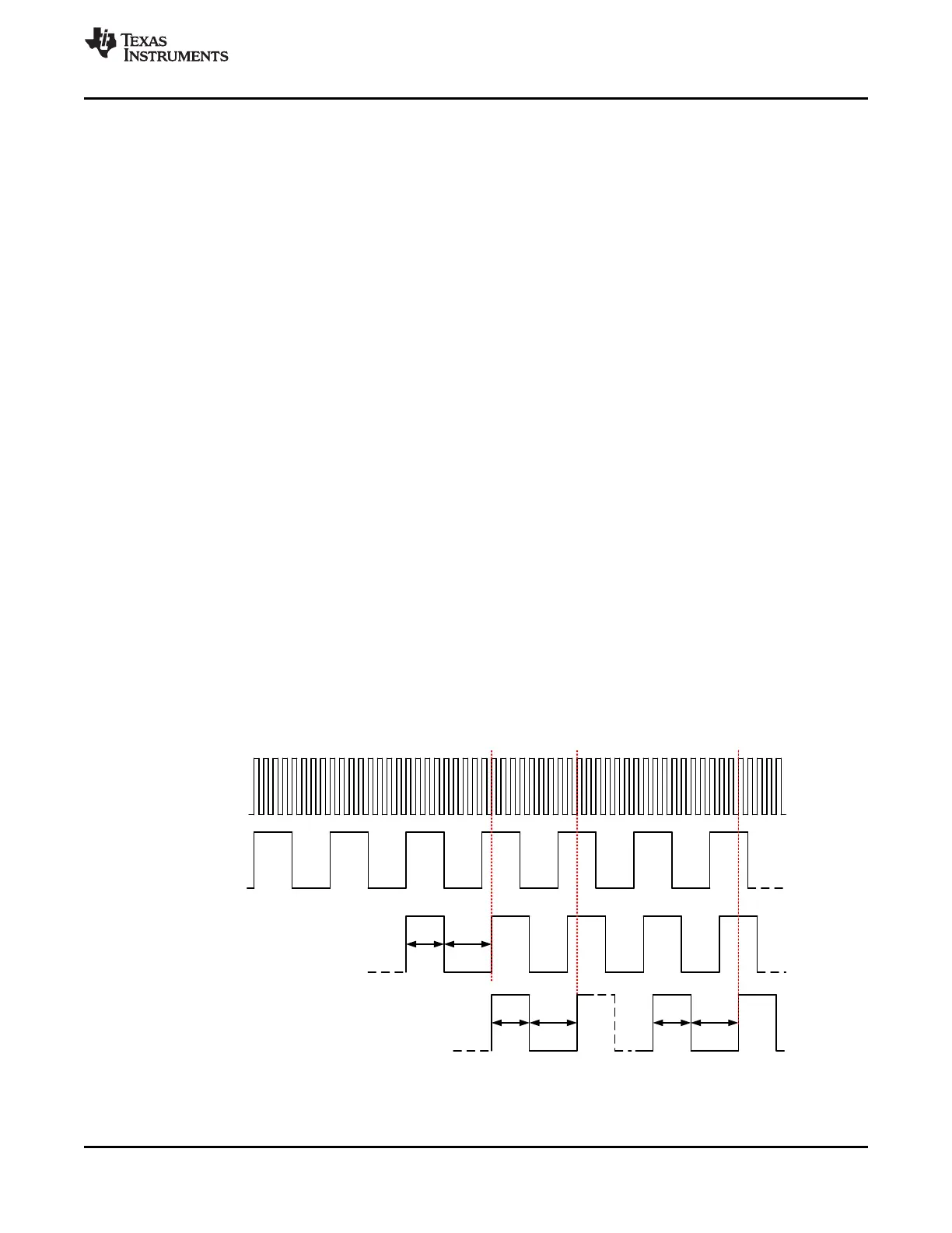
9.3.3.3 Single and Multiple Dynamic Digital Delay Example
In this example two separate adjustments will be made to the device clocks. In the first adjustment a single delay
of 1 VCO cycle will occur between DCLKout2 and DCLKout0. In the second adjustment two delays of 1 VCO
cycle will occur between DCLKout2 and DCLKout0. At this point in the example, DCLKout2 will be delayed 3
VCO cycles behind DCLKout0.
Assuming the device already has the following initial configurations:
• VCO frequency: 2949.12 MHz
• DCLKout0 = 368.64 MHz, DCLKout0_DIV = 8
• DCLKout2 = 368.64 MHz, DCLKout2_DIV = 8
The following steps illustrate the example above:
1. Set DCLKout2_DDLY_CNTH = 4. First part of delay for DCLKout2.
2. Set DCLKout2_DDLY_CNTL = 5. Second part of delay for DCLKout2.
3. Set DCLKout2_DDLY_PD = 0. Enable the digital delay for DCLKout2.
4. Set DDLYd2_EN = 1. Enable dynamic digital delay for DCLKout2.
5. Set SYNC_DIS0 = 1 and SYNC_DIS2 = 0. Sync should be disabled to DCLKout0, but not DCLKout2.
6. Set SYNC_MODE = 3. Enable SYNC event from SPI write to DDLYd_STEP_CNT's register.
7. Set SYNC_MODE = 2, SYSREF_MUX = 2. Setup proper SYNC settings.
8. Set DDLYd_STEP_CNT = 1. This begins the first adjustment.
Before step 8 DCLKout2 clock edge is aligned with DCLKout0.
After step 8, DCLKout2 counts four VCO cycles high and then five VCO cycles low as programmed by
DCLKout2_DDLY_CNTH and DCLKout2_DDLY_CNTL fields, effectively delaying DCLKout2 by one VCO cycle
with respect to DCLKout0. This is the first adjustment.
9. Set DDLYd_STEP_CNT = 2. This begins the second adjustment.
Before step 9, DCLKout2 clock edge was delayed 1 VCO cycle from DCLKout0.
After step 9, DCLKout2 counts four VCO cycles high and then five VCO cycles low as programmed by
DCLKout2_DDLY_CNTH and DCLKout2_DDLY_CNTL fields twice, delaying DCLKout2 by two VCO cycles with
respect to DCLKout0. This is the second adjustment.
Figure 15. Single and Multiple Adjustment Dynamic Digital Delay Example
Copyright © 2013–2015, Texas Instruments Incorporated Submit Documentation Feedback 41
Product Folder Links: LMK04821 LMK04826 LMK04828
 Loading...


