LMK04821
,
LMK04826
,
LMK04828
www.ti.com
SNAS605AR –MARCH 2013–REVISED DECEMBER 2015
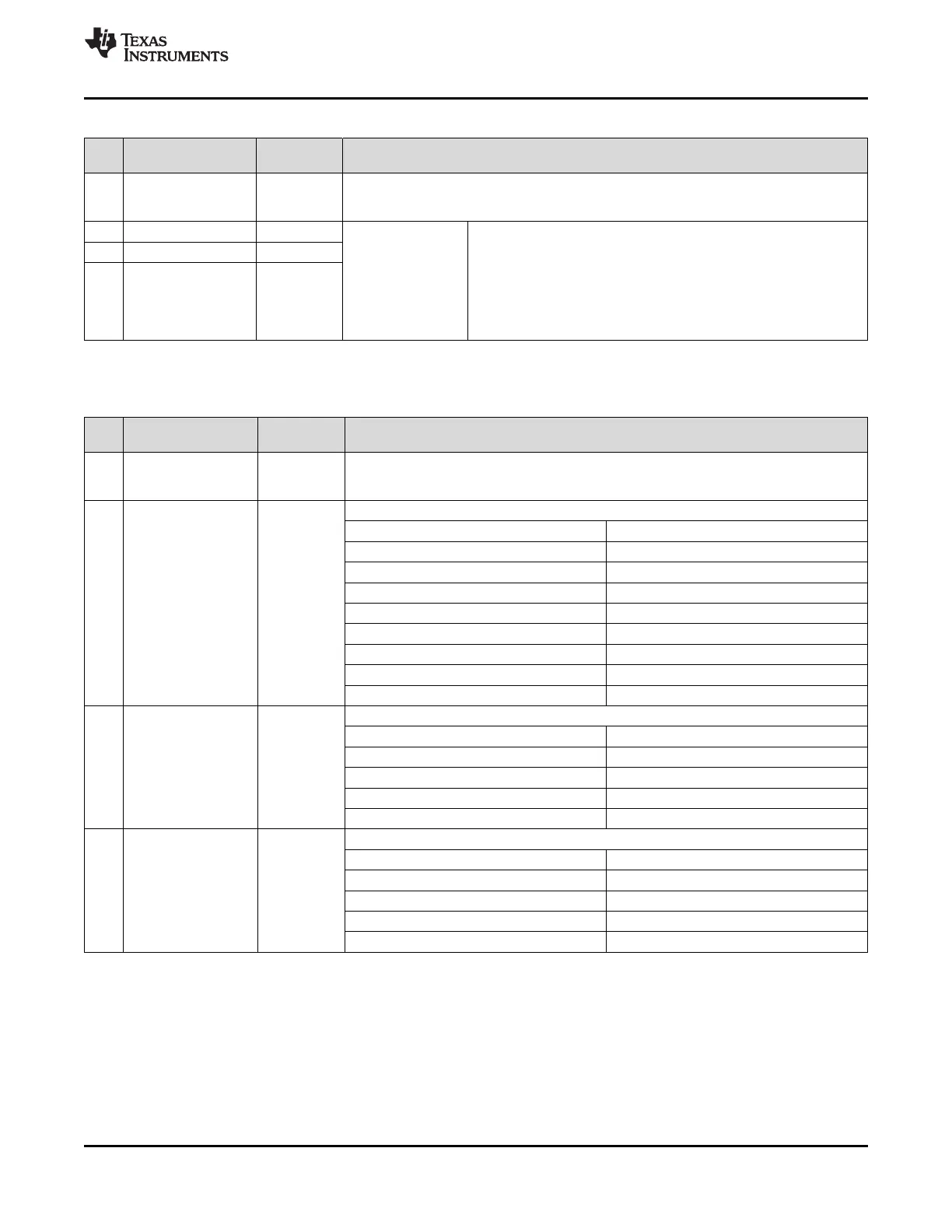
Table 37. Register 0x146 (continued)
BIT POR
NAME DESCRIPTION
DEFAULT
Enable CLKin0 to be used during auto-switching of CLKin_SEL_MODE.
3 CLKin0_EN 1 0: Not enabled for auto mode
1: Enabled for auto mode
2 CLKin2_TYPE 0 There are two buffer types for CLKin0, 1, and 2: bipolar and CMOS.
Bipolar is recommended for differential inputs like LVDS or LVPECL.
1 CLKin1_TYPE 0
CMOS is recommended for DC coupled single ended inputs.
0: Bipolar When using bipolar, CLKinX and CLKinX* must be AC coupled.
1: MOS When using CMOS, CLKinX and CLKinX* may be AC or DC coupled
0 CLKin0_TYPE 0
if the input signal is differential. If the input signal is single-ended the
used input may be either AC or DC coupled and the unused input
must AC grounded.
9.7.4.2 CLKin_SEL_POL, CLKin_SEL_MODE, CLKin1_OUT_MUX, CLKin0_OUT_MUX
Table 38. Register 0x147
POR
BIT NAME DESCRIPTION
DEFAULT
Inverts the CLKin polarity for use in pin select mode.
7 CLKin_SEL_POL 0 0: Active High
1: Active Low
Sets the mode used in determining the reference for PLL1.
Field Value CLKin Mode
0 (0x00) CLKin0 Manual
1 (0x01) CLKin1 Manual
2 (0x02) CLKin2 Manual
6:4 CLKin_SEL_MODE 3
3 (0x03) Pin Select Mode
4 (0x04) Auto Mode
5 (0x05) Reserved
6 (0x06) Reserved
7 (0x07) Reserved
Selects where the output of the CLKin1 buffer is directed.
Field Value CLKin1 Destination
0 (0x00) Fin
3:2 CLKin1_OUT_MUX 2
1 (0x01) Feedback Mux (0-delay mode)
2 (0x02) PLL1
3 (0x03) Off
Selects where the output of the CLKin0 buffer is directed.
Field Value CLKin0 Destination
0 (0x00) SYSREF Mux
1:0 CLKin0_OUT_MUX 2
1 (0x01) Reserved
2 (0x02) PLL1
3 (0x03) Off
Copyright © 2013–2015, Texas Instruments Incorporated Submit Documentation Feedback 69
Product Folder Links: LMK04821 LMK04826 LMK04828
 Loading...


