V
A
V
B
GND
V
OD
= | V
A
- V
B
|
V
SS
= 2·V
OD
V
OD
Definition V
SS
Definition for Output
Non-Inverting Clock
Inverting Clock
V
OD
2·V
OD
V
A
V
B
GND
V
ID
= | V
A
- V
B
|
V
SS
= 2·V
ID
V
ID
Definition V
SS
Definition for Input
Non-Inverting Clock
Inverting Clock
V
ID
2·V
ID
LMK04821
,
LMK04826
,
LMK04828
www.ti.com
SNAS605AR –MARCH 2013–REVISED DECEMBER 2015
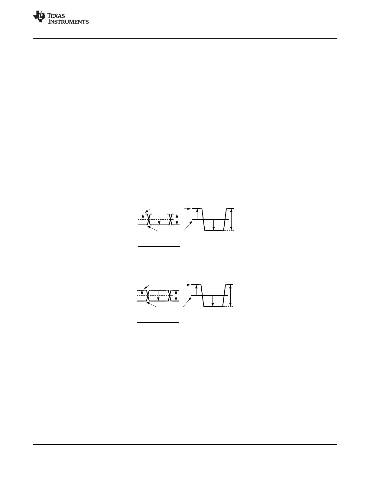
8.2 Differential Voltage Measurement Terminology
The differential voltage of a differential signal can be described by two different definitions causing confusion
when reading data sheets or communicating with other engineers. This section will address the measurement
and description of a differential signal so that the reader will be able to understand and distinguish between the
two different definitions when used.
The first definition used to describe a differential signal is the absolute value of the voltage potential between the
inverting and non-inverting signal. The symbol for this first measurement is typically V
ID
or V
OD
depending on if
an input or output voltage is being described.
The second definition used to describe a differential signal is to measure the potential of the non-inverting signal
with respect to the inverting signal. The symbol for this second measurement is V
SS
and is a calculated
parameter. Nowhere in the IC does this signal exist with respect to ground, it only exists in reference to its
differential pair. V
SS
can be measured directly by oscilloscopes with floating references, otherwise this value can
be calculated as twice the value of V
OD
as described in the first description.
Figure 8 illustrates the two different definitions side-by-side for inputs and Figure 9 illustrates the two different
definitions side-by-side for outputs. The V
ID
and V
OD
definitions show V
A
and V
B
DC levels that the non-inverting
and inverting signals toggle between with respect to ground. V
SS
input and output definitions show that if the
inverting signal is considered the voltage potential reference, the non-inverting signal voltage potential is now
increasing and decreasing above and below the non-inverting reference. Thus the peak-to-peak voltage of the
differential signal can be measured.
V
ID
and V
OD
are often defined as volts (V) and V
SS
is often defined as volts peak-to-peak (V
PP
).
Figure 8. Two Different Definitions for
Differential Input Signals
Figure 9. Two Different Definitions for
Differential Output Signals
Refer to application note AN-912 Common Data Transmission Parameters and their Definitions (SNLA036) for
more information.
Copyright © 2013–2015, Texas Instruments Incorporated Submit Documentation Feedback 27
Product Folder Links: LMK04821 LMK04826 LMK04828
 Loading...


