0.2 mm
1.46 mm
7.2 mm
1.15 mm
LMK04821
,
LMK04826
,
LMK04828
www.ti.com
SNAS605AR –MARCH 2013–REVISED DECEMBER 2015
12 Layout
12.1 Layout Guidelines
12.1.1 Thermal Management
Power consumption of the LMK0482x family of devices can be high enough to require attention to thermal
management. For reliability and performance reasons the die temperature should be limited to a maximum of
125°C. That is, as an estimate, T
A
(ambient temperature) plus device power consumption times R
θJA
should not
exceed 125°C.
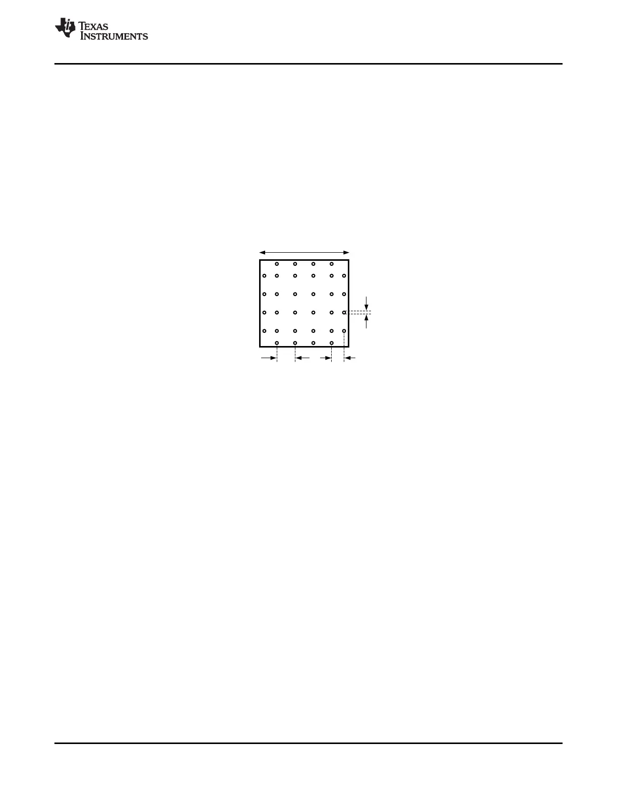
The package of the device has an exposed pad that provides the primary heat removal path as well as excellent
electrical grounding to a printed circuit board. To maximize the removal of heat from the package a thermal land
pattern including multiple vias to a ground plane must be incorporated on the PCB within the footprint of the
package. The exposed pad must be soldered down to ensure adequate heat conduction out of the package.
Figure 33. Recommended Land and Via Pattern
Copyright © 2013–2015, Texas Instruments Incorporated Submit Documentation Feedback 103
Product Folder Links: LMK04821 LMK04826 LMK04828
 Loading...


