LMK04821
,
LMK04826
,
LMK04828
SNAS605AR –MARCH 2013–REVISED DECEMBER 2015
www.ti.com
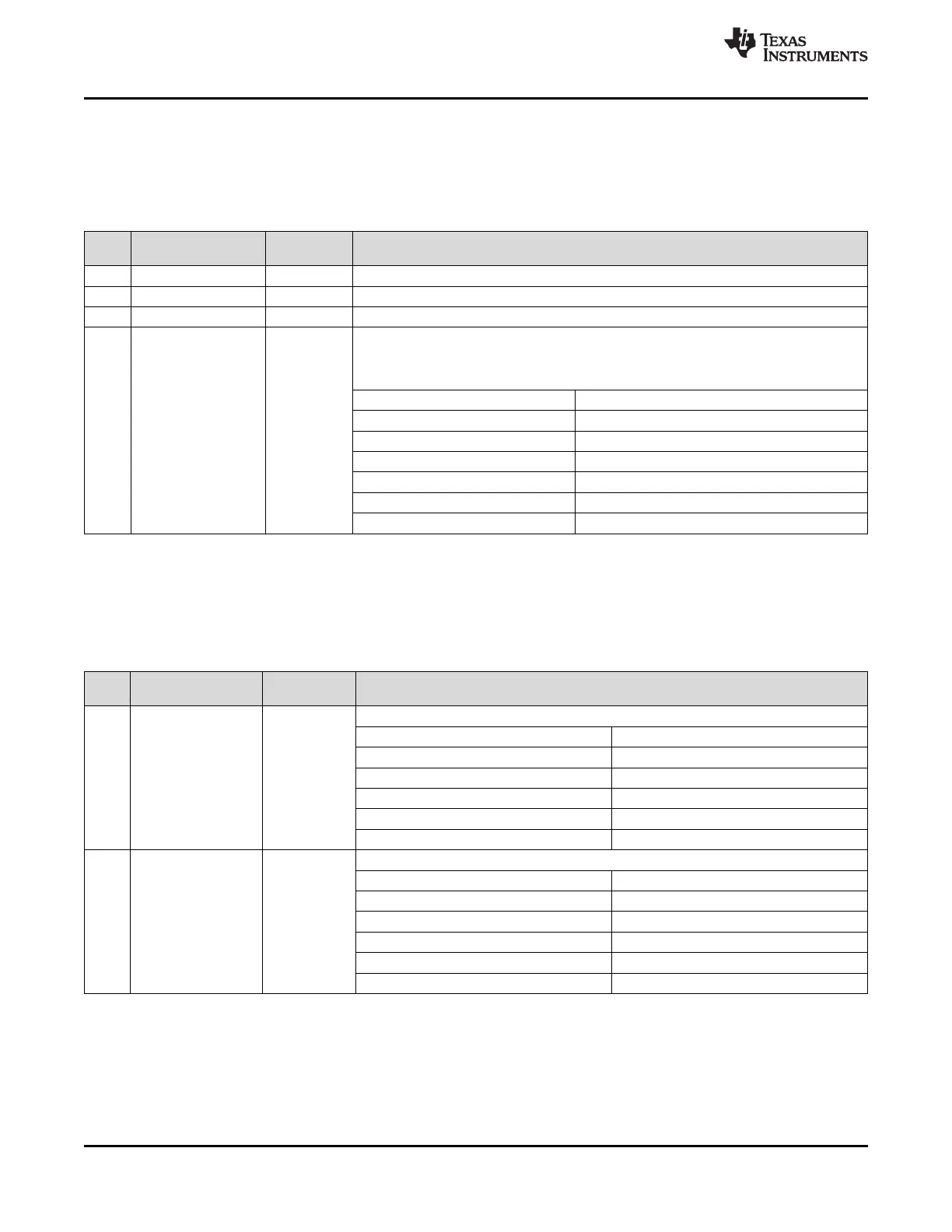
9.7.2 (0x100 - 0x138) Device Clock and SYSREF Clock Output Controls
9.7.2.1 CLKoutX_Y_ODL, CLKoutX_Y_IDL, DCLKoutX_DIV
These registers control the input and output drive level as well as the device clock out divider values.
Table 16. Registers 0x100, 0x108, 0x110, 0x118, 0x120, 0x128, and 0x130
POR
BIT NAME DESCRIPTION
DEFAULT
7 NA 0 Reserved
6 CLKoutX_Y_ODL 0 Output drive level.
5 CLKoutX_Y_IDL 0 Input drive level.
DCLKoutX_DIV sets the divide value for the clock output, the divide may be even or odd.
Both even or odd divides output a 50% duty cycle clock if duty cycle correction (DCC) is
selected.
Divider is unused if DCLKoutX_MUX = 2 (bypass), equivalent divide of 1.
X = 0 → 2
Field Value Divider Value
X = 2 → 4
X = 4 → 8
0 (0x00) 32
4:0 DCLKoutX_DIV X = 6 → 8
1 (0x01) 1
(1)
X = 8 → 8
X = 10 → 8
2 (0x02) 2
X = 12 → 2
... ...
30 (0x1E) 30
31 (0x1F) 31
(1) Not valid if DCLKoutX_MUX = 0, Divider only. Not valid if DCLKoutX_MUX = 3 (Analog Delay + Divider) and DCLKoutX_ADLY_MUX =
0 (without duty cycle correction/halfstep).
9.7.2.2 DCLKoutX_DDLY_CNTH, DCLKoutX_DDLY_CNTL
This register controls the digital delay high and low count values for the device clock outputs.
Table 17. Registers 0x101, 0x109, 0x111, 0x119, 0x121, 0x129, 0x131
POR
BIT NAME DESCRIPTION
DEFAULT
Number of clock cycles the output will be high when digital delay is engaged.
Field Value Delay Values
0 (0x00) 16
DCLKoutX
7:4 5 1 (0x01) Reserved
_DDLY_CNTH
2 (0x02) 2
... ...
15 (0x0F) 15
Number of clock cycles the output will be low when dynamic digital delay is engaged.
Field Value Delay Values
0 (0x00) 16
DCLKoutX
3:0 5 1 (0x01) Reserved
_DDLY_CNTL
2 (0x02) 2
... ...
15 (0x0F) 15
56 Submit Documentation Feedback Copyright © 2013–2015, Texas Instruments Incorporated
Product Folder Links: LMK04821 LMK04826 LMK04828
 Loading...


