LMK04821
,
LMK04826
,
LMK04828
SNAS605AR –MARCH 2013–REVISED DECEMBER 2015
www.ti.com
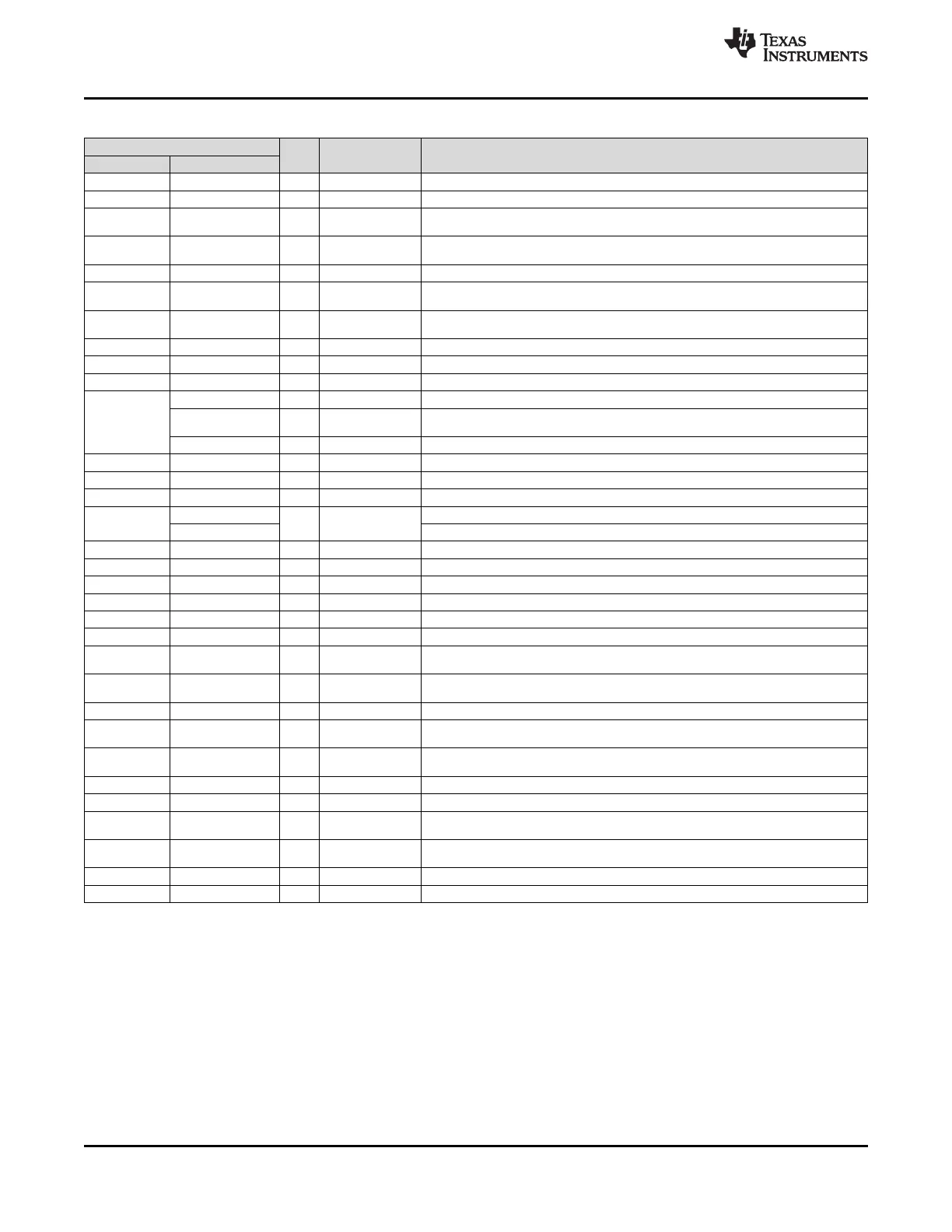
Pin Functions (continued)
PIN
I/O TYPE DESCRIPTION
(1)
NO. NAME
20 SDIO I/O CMOS SPI Data
21 Vcc3_SYSREF PWR Power supply for SYSREF divider and SYNC.
SDCLKout5,
22, 23 O Programmable SYSREF / Device clock output 5.
SDCKLout5*
DCLKout4,
24, 25 O Programmable Device clock output 4.
DCLKout4*
26 Vcc4_CG2 PWR Power supply for clock outputs 4, 5, 6 and 7.
DCLKout6,
27, 28 O Programmable Device clock output 6.
DCLKout6*
SDCLKout7,
29, 30 O Programmable SYSREF / Device clock output 7.
SDCLKout7*
31 Status_LD1 I/O Programmable Programmable status pin.
32 CPout1 O ANLG Charge pump 1 output.
33 Vcc5_DIG PWR Power supply for the digital circuitry.
CLKin1, CLKin1* I ANLG Reference Clock Input Port 1 for PLL1.
FBCLKin,
34, 35 I ANLG Feedback input for external clock feedback input (0–delay mode).
FBCLKin*
Fin, Fin* I ANLG External VCO Input (External VCO mode).
36 Vcc6_PLL1 PWR Power supply for PLL1, charge pump 1, holdover DAC
37, 38 CLKin0, CLKin0* I ANLG Reference Clock Input Port 0 for PLL1.
39 Vcc7_OSCout PWR Power supply for OSCout port.
OSCout, OSCout* Buffered output of OSCin port.
40, 41 I/O Programmable
CLKin2, CLKin2* Reference Clock Input Port 2 for PLL1.
42 Vcc8_OSCin PWR Power supply for OSCin
43, 44 OSCin, OSCin* I ANLG Feedback to PLL1, Reference input to PLL2. AC coupled.
45 Vcc9_CP2 PWR Power supply for PLL2 Charge Pump.
46 CPout2 O ANLG Charge pump 2 output.
47 Vcc10_PLL2 PWR Power supply for PLL2.
48 Status_LD2 I/O Programmable Programmable status pin.
SDCLKout9,
49, 50 O Programmable SYSREF / Device clock 9
SDCLKout9*
DCLKout8,
51, 52 O Programmable Device clock output 8.
DCLKout8*
53 Vcc11_CG3 PWR Power supply for clock outputs 8, 9, 10, and 11.
DCLKout10,
54, 55 O Programmable Device clock output 10.
DCLKout10*
SDCLKout11,
56, 57 O Programmable SYSREF / Device clock output 11.
SDCLKout11*
58 CLKin_SEL0 I/O Programmable Programmable status pin.
59 CLKin_SEL1 I/O Programmable Programmable status pin.
SDCLKout13,
60, 61 O Programmable SYSREF / Device clock output 13.
SDCLKout13*
DCLKout12,
62, 63 O Programmable Device clock output 12.
DCLKout12*
64 Vcc12_CG0 PWR Power supply for clock outputs 0, 1, 12, and 13.
DAP DAP GND DIE ATTACH PAD, connect to GND.
8 Submit Documentation Feedback Copyright © 2013–2015, Texas Instruments Incorporated
Product Folder Links: LMK04821 LMK04826 LMK04828
 Loading...


