RM23712 TPS
34
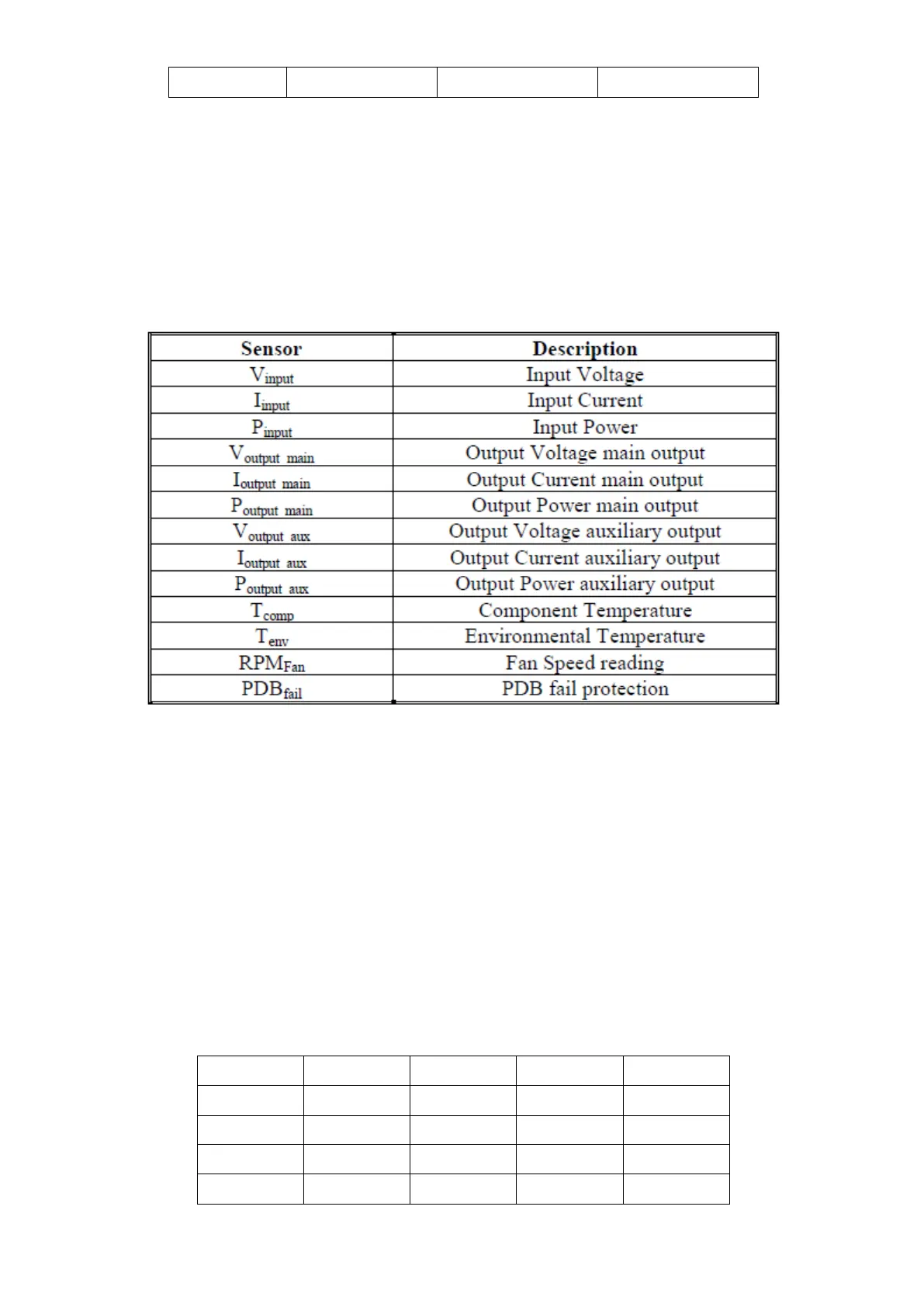
3.4.2.8 PSMC Sensors
Sensors shall be available to the PSMC for monitoring purpose.
All Sensors shall continue to provide real time data as long as the PSMC device is powered.
This means in standby and operation mode, while in standby the main output(s) of the power supply
shall read zero Amps and Volts.
Table 36.PSMC Sensor list
3.4.3 Power Supply Field Replacement Unit (FRU)
The power supply shall support electronic access of FRU information over an I
2
C bus. Six pins at
the power supply connector are allocated for this. They are named SCL, SDA, A1, A0 and Write
protect. SCL is serial clock. SDA is serial data. These two bidirectional signals from the basic
communication lines over the I
2
C bus. A0 and A1 are input address lines to the power supply. The
backplane defines the state of these lines such that the address to the power supply is unique within
the system. The resulting I
2
C address shall be per table below. The Write protection pin is to
ensure that data will not accidentally overwritten.
The device used for this shall be powered from a 3.3V bias voltage derived from the +12 Vsb output .
The pull-up resistors shall be on SCL or SDA inside the power supply.
Table 37.Sensor Accuracy
 Loading...