95
DST1-ID12SL-1 Section 5-1
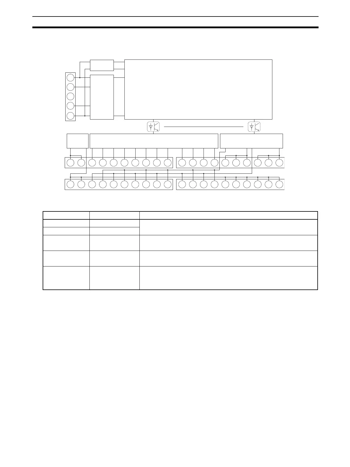
5-1-4 Internal Circuits and Terminal Arrangement
The following figure shows the internal circuits of the DST1-ID12SL-1.
The following table gives the terminal arrangement of the terminal blocks on
the DST1-ID12SL-1.
V
G
V
G
IN1
T1
IN0
T0
IN3
T1
IN2
T0
IN5
T1
IN4
T0
IN7
T1
IN6
T0
IN8
T0
IN9
T1
IN
11
T1
IN
10
T0
T2
G
T2
G
T3
G
T2
G
T3
G
T3
G
CAN
H
V−
V+
CAN
L
12345678910
11 12 13 14 15 16 17 18 19 20
21 22 23 24 25 26 27 28 29 30
31 32 33 34 35 36 37 38 39 40
Safety input circuits
(current sinking)
DC-DC
converter
(non-isolated)
DeviceNet
physical
layer
I/O power
supply
circuit
Internal circuits
Test output circuits
(current sourcing)
Shield
Terminals Names Functions
1, 2 V Power terminals for the input devices and test outputs. (24 VDC)
11, 12 G
35 to 40 G Common terminals
The terminals 11, 12 and 35 to 40 are internally connected.
3 to 10
21 to 24
IN0 to IN11 Terminals for safety inputs
13 to 20
25 to 30
31 to 34
T0 to T3 Terminals for test outputs
 Loading...