I
•NTENSITY
I
Vertical
Chopped
Blanking Signal
from Vertical Switching
Circuit
External Blanking
from Z
AXIS
INPUT
Connector
A
and
B
unblanking
gate
from
Sweep
Generator
circuits
R1005
R1004
R1011
R1012
C1036
Circuit
Description-Type
453/R453
+
90
V to
r------"~
Geometry
Adjustment
Unblanking
gate
to
CRT
circuit
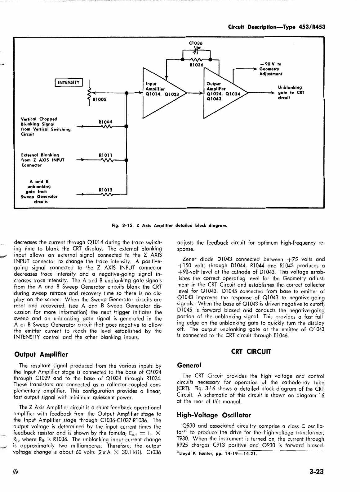
Fig.
3-15.
Z Axis Amplifier
detailed
block
diagram.
decreases the current through
Ql
014
during the trace switch-
ing time to blank the
CRT
display.
The
external blanking
input allows an external signal connected to the Z
AXIS
INPUT
connector to change the trace intensity. A positive-
going signal connected to the Z
AXIS
INPUT
connector
decreases trace intensity and a negative-going signal
in-
creases trace intensity.
The
A and B unblanking
gate
signals
from
the A and B Sweep Generator circuits blank the
CRT
during sweep retrace and recovery time
so
there
is
no
dis-
play on the screen. When the Sweep Generator circuits
are
reset and recovered,
(see
A and B Sweep Generator dis-
cussion for more information) the next trigger initiates the
sweep and an unblanking gate signal
is
generated
in
the
A or B Sweep Generator circuit that goes negative to allow
the emitter current to reach the
level
established by the
INTENSITY
control and the other blanking inputs.
Output
Amplifier
The
resultant signal produced
from
the various inputs by
the Input Amplifier stage
is
connected to the base of
Ql
024
through
Cl
029
and to the base of
Ql
034 through
Rl
024.
These transistors are connected as a collector-coupled
com-
plementary amplifier.
This
configuration provides a linear,
fast output signal
with
minimum
quiescent power.
The
Z
Axis
Amplifier circuit
is
a shunt-feedback operational
amplifier
with
feedback
from
the Output Amplifier stage to
the Input Amplifier stage through
Cl
036-Cl
037-Rl
036.
The
output voltage
is
determined by the input current
times
the
feedback resistor and
is
shown by the fomula· E t -
i·
X
Rtb
where
Rtb
is
Rl
036.
The
unblanking input
~ur~uen~h~nge
is
approximately two milliamperes. Therefore, the output
voltage change
is
about
60
volts
(2
mA
X
30.
l kn).
Cl
036
®
adjusts the feedback circuit for optimum high-frequency
re-
sponse.
Zener diode
Dl
043
conneded between
+75
volts and
+
150
volts through
Dl
044,
Rl
044 and
Rl
043
produces a
+90-volt
level
at
the cathode of
Dl
043.
This
voltage estab-
lishes
the correct operating
level
for the Geometry adjust-
ment
in
the
CRT
Circuit and establishes the correct collector
level
for
Ql
043.
Dl
045 connected
from
base to emitter of
<?1043
improves the response of Ql043
to
negative-going
signals. When the base of
Ql
043
is
driven negative
to
cutoff,
Dl
045
is
forward biased and conducts the negative-going
portion of the unblanking signal.
This
provides a fast fall-
ing
edge
on
the unblanking gate
to
quickly turn the display
off.
The
output unblanking gate
at
the emitter of
Ql
043
is
connected to the
CRT
circuit through
Rl
046.
CRT
CIRCUIT
General
The
CRT
Circuit provides the
high
voltage and control
circuits necessary for operation of the cathode-ray tube
(CRT).
Fig.
3-16 shows a detailed block diagram of the
CRT
Circuit. A schematic of
this
circuit
is
shown
on
diagram
16
at
the rear of
this
manual.
High-Voltage Oscillator
0930
and associated circuitry comprise a class C oscilla-
tor10
to produce the drive for the high-voltage transformer,
T930.
When the instrument
is
turned
on,
the current through
R925
charges
C913
positive and Q930
is
forward biased.
10
Lloyd
P.
Hunter,
pp.
14-19-14-21.
3-23
 Loading...