Circuit
Description-Type
453/R453
6.3-Volt
RMS
AC Source
The
6.3-volt
RMS
secondary winding of
Tl
l
01
provides
power for the
POWER
ON
light,
Bl
l
07,
and the scale
illu-
mination lights,
Bl
l
08
and
Bl
l
09.
The
current through the
scale illumination lights
is
controlled by the
SCALE
ILLUM
control,
Rl
l
08,
to change the illumination of the graticule
line
voltage to the A and B Trigger Generator circuits for
line voltage to the A and B Trigger Generaor circuits for
internal triggering
at
the line frequency.
Cl
l
05
reduces
noise on the line frequency signal.
VOLTAGE DISTRIBUTION
Diagram 17 also shows the distribution of the output volt-
ages
from
the Power Supply circuit to the circuit boards
in
this
instrument.
The
decoupling networks which provide de-
coupled operating voltages
are
shown on
this
Diagram and
are
not repeated on the individual circuit diagrams.
CALIBRATOR
General
The
Calibrator circuit produces a square-wave output
with
accurate amplitude and frequency.
This
output
is
available
as a square-wave voltage
at
the l
kHz
CAL
connector or
as a square-wave current through the side-panel
PROBE
LOOP.
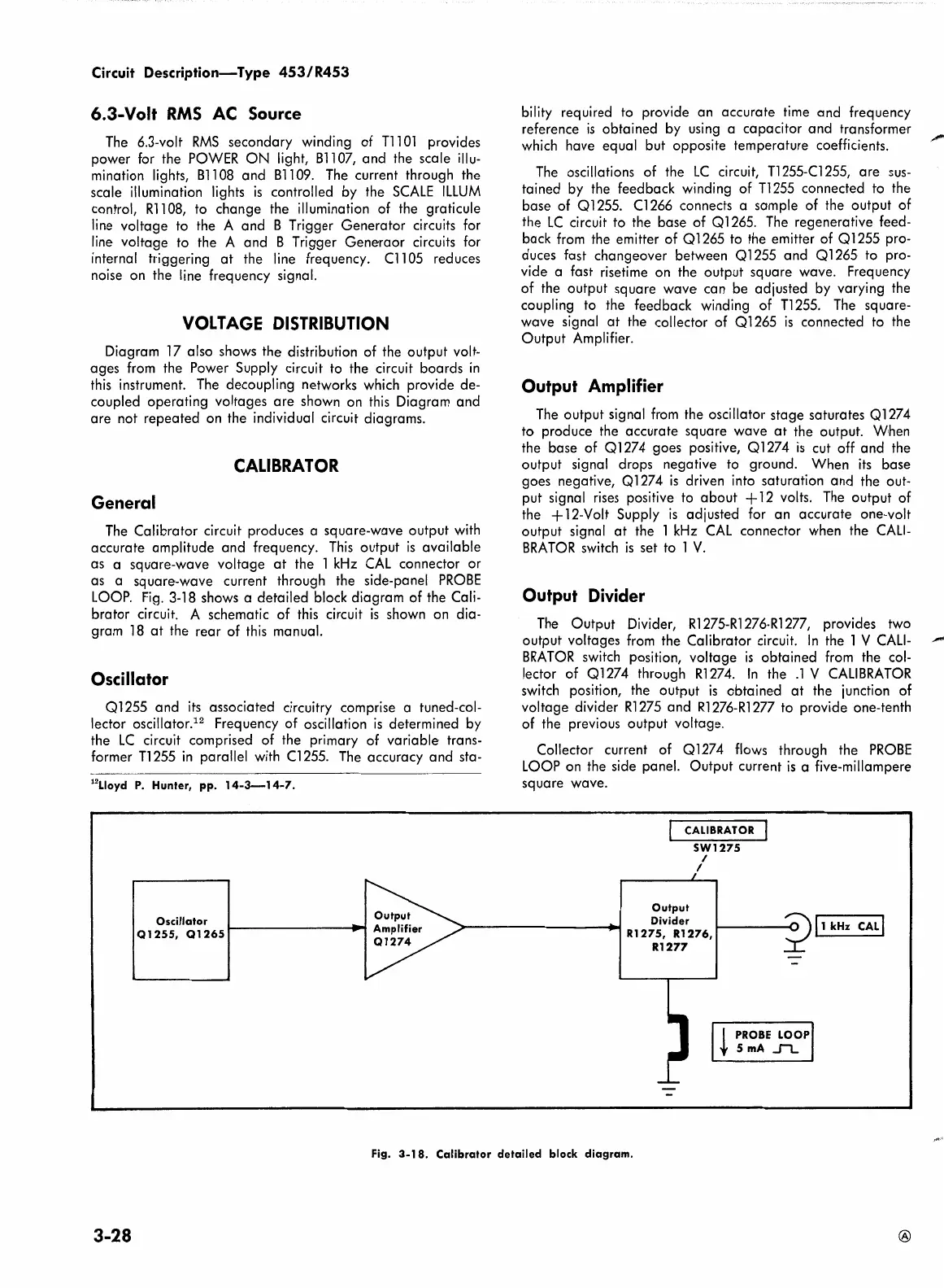
Fig.
3-18 shows a detailed block diagram of the Cali-
brator circuit. A schematic of
this
circuit
is
shown on dia-
gram
18
at
the rear of
this
manual.
Oscillator
Ql
255 and
its
associated circuitry comprise a tuned-col-
lector oscillator.
12
Frequency of oscillation
is
determined by
the
LC
circuit comprised of the primary of variable trans-
former
Tl
255
in
parallel
with
Cl
255.
The
accuracy and sta-
12
Lloyd
P.
Hunter,
pp.
14-3-14-7.
Oscillator
Q1255,
Q1265
bility required to provide an accurate time and frequency
reference
is
obtained by
using
a capacitor and transformer
which have equal but opposite temperature coefficients.
The
oscillations of the
LC
circuit,
Tl
255-Cl
255,
are
sus-
tained by the feedback winding of
Tl
255
connected to the
base of
Ql
255.
Cl
266
connects a sample of the output of
the
LC
circuit to the base of
Ql
265.
The
regenerative feed-
back
from
the emitter of
Ql
265
to the emitter of
Ql
255 pro-
duces fast changeover between
Ql
255
and
Ql
265
to pro-
vide a fast risetime on the output square wave. Frequency
of the output square wave can be adjusted by varying the
coupling to the feedback winding of
Tl
255.
The
square-
wave signal
at
the collector of
Ql
265
is
connected to the
Output Amplifier.
Output
Amplifier
The
output signal
from
the oscillator stage saturates
Ql
27
4
to produce the accurate square wave
at
the output. When
the base of
Ql274
goes positive,
Ql274
is
cut off and the
output signal drops negative to ground. When
its
base
goes negative,
Ql
27
4
is
driven into saturation and the out-
put signal
rises
positive to about +
12
volts.
The
output of
the
+ 12-Volt Supply
is
adjusted for an accurate one-volt
output signal
at
the l
kHz
CAL
connector when the
CALI-
BRATOR
switch
is
set to l
V.
Output Divider
The
Output Divider,
Rl
275-Rl
276-Rl
277,
provides two
output voltages
from
the Calibrator circuit.
In
the 1 V
CALI-
BRATOR
switch position, voltage
is
obtained
from
the col-
lector of
Ql274
through Rl274.
In
the .l V
CALIBRATOR
switch position, the output
is
obtained
at
the junction of
voltage divider
Rl
275
and
Rl
276-Rl
277 to provide one-tenth
of the previous output voltage.
Collector current of
Ql
27
4
flows
through the
PROBE
LOOP
on the side panel. Output current
is
a five-millampere
square wave.
CALIBRATOR
SW1275
Output
Divider
I
I
Rl
275,
Rl
276,
R1277
I
PROBE
LOOP
'f
5 mA
fl...
Fig.
3-18.
Calibrator
detailed
block
diagram.
3-28
®
 Loading...