2GM
2-3-26
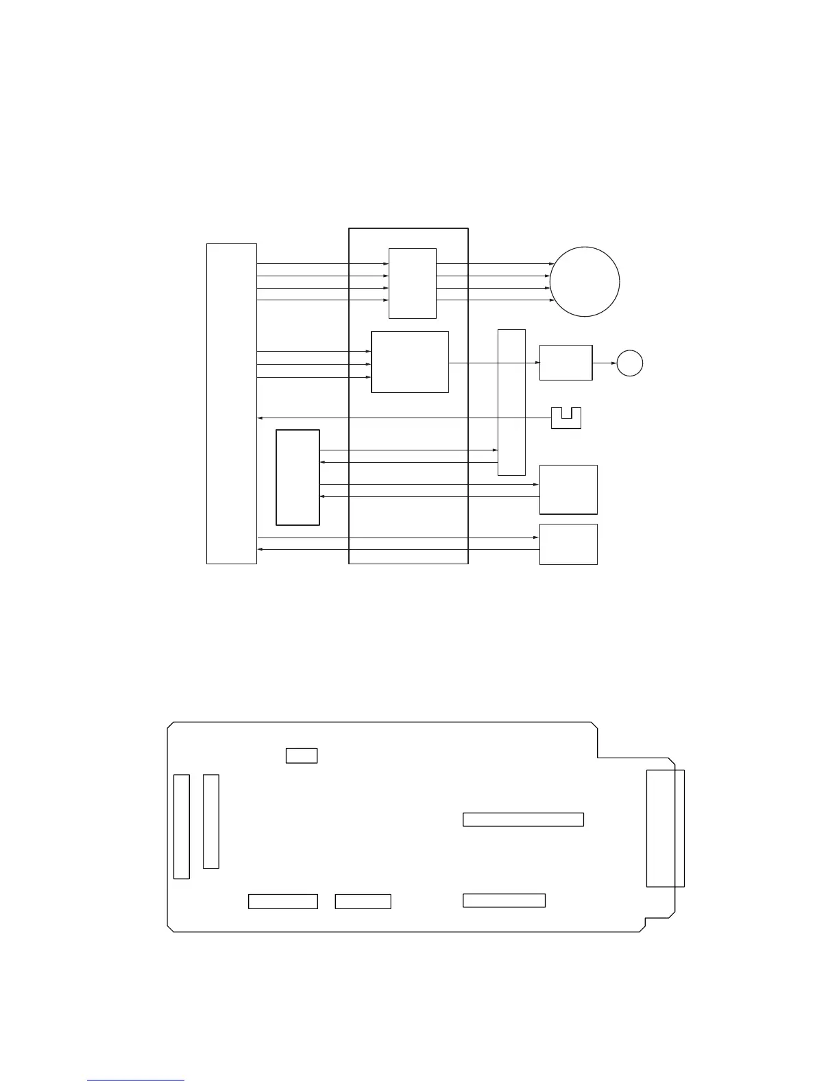
Figure 2-3-20 Scanner PWB circuit block diagram
Operation
PWB
Inverter
PWB
Scanner PWB
Optional
DP
Main
PWB
Engine
PWB
Driver
circuit
(U1)
Exposure
lamp driver
circuit
(Q1, 2, 3, 4, 5)
Scanner
motor
CCD PWB
Exposure
lamp
Scanner
home
position
switch
MOTA
MOTNA
MOTB
LAMP
LAMPHI
LAMPLOW
HPSWN
MOTNB
ISUMOTA
ISUMOTNA
ISUMOTB
ISUMOTNB
2-3-8 Scanner PWB
The scanner PWB consists of scanner driver circuit Q1 to Q5 and exposure lamp driver circuit U1, relays signals from
engine PWB, main PWB, operation PWB, CCD PWB and optional document processor.
YC5
120
118
15 1
YC4
YC8
YC3
113
YC2
YC1
YC7
YC6
1
1
130
4
10
120
Figure 2-3-21 Scanner PWB silk-screen diagram
 Loading...