XBee® Wi-Fi RF Modules
© 2013 Digi International, Inc. 18
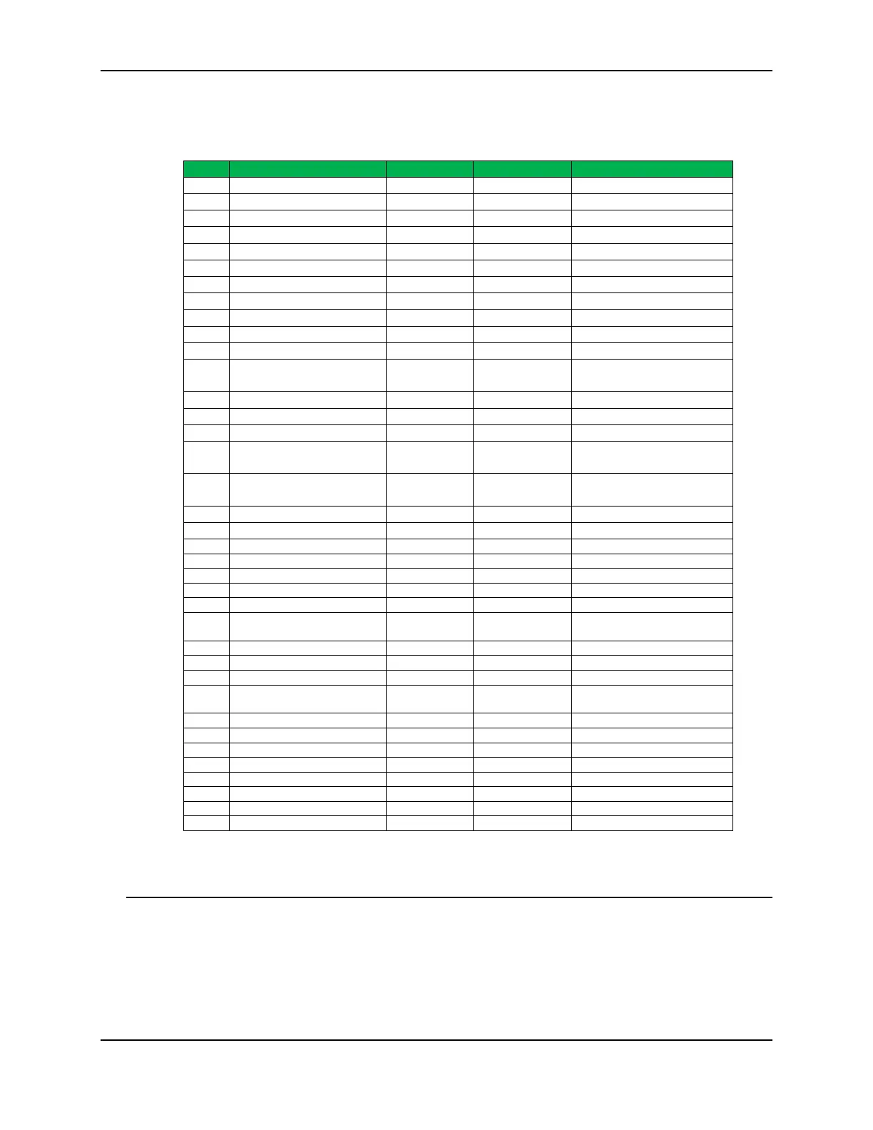
Pin Assignment for the XBee Wi-Fi Surface Mount module
(Low-asserted signals are distinguished with a lower case n before the signal name.)
Pin # Name Direction Default State Description
1 GND - - Ground
2 VCC - - Power Supply
3 DIO13/DOUT Both Output UART Data Out
4 DIO14/DIN/nCONFIG Both Input UART Data In
5 DIO12 Both Disabled GPIO
6 nRESET Input Input Module Reset
7 DIO10/PWM0 Both Disabled GPIO
8 DIO11/PWM1 Both Disabled GPIO
9 Reserved - - Do Not Connect
10 DIO8/nDTR/SLEEP_RQ Both Input GPIO
11 GND - - Ground
12 DIO19/SPI_nATTN Both Output GPIO/SPI Attention
13 GND - - Ground
14 DIO18/SPI_CLK Both Input GPIO/SPI Clock
15 DIO17/SPI_nSSEL Both Input GPIO/SPI Slave Select
16 DIO16/SPI_SI Both Input GPIO/SPI Slave In
17 DIO15/SPI_SO Both Output GPIO/SPI Slave Out
18 Reserved - - Do Not Connect
19 Reserved - - Do Not Connect
21 Reserved - - Do Not Connect
22 GND - - Ground
23 Reserved - - Do Not Connect
25 DIO7/nCTS Both Output
Clear-to-Send Flow Control/
26 DIO9/On_nSLEEP Both Output Module Status Indicator/GPIO
27 VREF - - Not connected
28 DIO5/ASSOC Both Output Associate Indicator/GPIO
29 DIO6/nRTS Both Input
Request-to-Send Flow Control/
30 DIO3/AD3 Both Disabled Analog Input/GPIO
31 DIO2/AD2 Both Disabled Analog Input/GPIO
32 DIO1/AD1 Both Disabled Analog Input/GPIO
34 Reserved - - Do Not Connect
35 GND - - Ground
36 RF Both - RF IO for RF Pad Variant
Design Notes
XBee modules are designed to be self sufficient and do not specifically require any
external circuitry other than the recommended pin connections described below.
The
following sections discuss general design guidelines that are recommended for help in
troubleshooting and building a robust design.
 Loading...