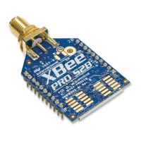
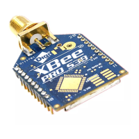
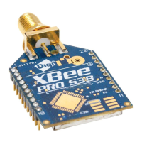
XBee® Wi-Fi RF Modules
© 2013 Digi International, Inc. 23
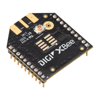
Design Notes for RF Pad
The RF Pad is a soldered antenna connection. The RF signal travels from pin 36 on the
module to the antenna through an RF trace transmission line on the PCB. Please note
that any additional components between the module and antenna will violate modular
certification. The RF trace should have a controlled impedance of 50 ohms. We
recommend using a microstrip trace, although coplanar waveguide may also be used if
more isolation is needed. Microstrip generally requires less area on the PCB than
coplanar waveguide. Stripline is not recommended because sending the signal to
different PCB layers can introduce matching and performance problems.
It is essential to follow good design practices when implementing the RF trace on a PCB.
The following figures show a layout example of a host PCB that connects an RF Pad
module to a right angle, through-hole RPSMA jack. The top two layers of the PCB have a
controlled thickness dielectric material in between. The second layer has a ground plane
which runs underneath the entire RF Pad area. This ground plane is a distance d, the
thickness of the dielectric, below the top layer. The top layer has an RF trace running
from pin 36 of the module to the RF pin of the RPSMA connector. The RF trace's width
determines the impedance of the transmission line with relation to the ground plane.
Many online tools can estimate this value, although the PCB manufacturer should be
consulted for the exact width. Assuming d=0.025", and that the dielectric has a relative
permittivity of 4.4, the width in this example will be approximately 0.045" for a 50 ohm
trace. This trace width is a good fit with the module footprint's 0.060" pad width. Using
a trace wider than the pad width is not recommended, and using a very narrow trace
(under 0.010") can cause unwanted RF loss. The length of the trace is minimized by
placing the RPSMA jack close to the module. All of the grounds on the jack and the
module are connected to the ground planes directly or through closely placed vias. Any
ground fill on the top layer should be spaced at least twice the distance d (in this case, at
least 0.050") from the microstrip to minimize their interaction.
Implementing these design suggestions will help ensure that the RF Pad module
performs to its specifications.
 Loading...