2-26 Service Manual
5025-2xx, 4xx
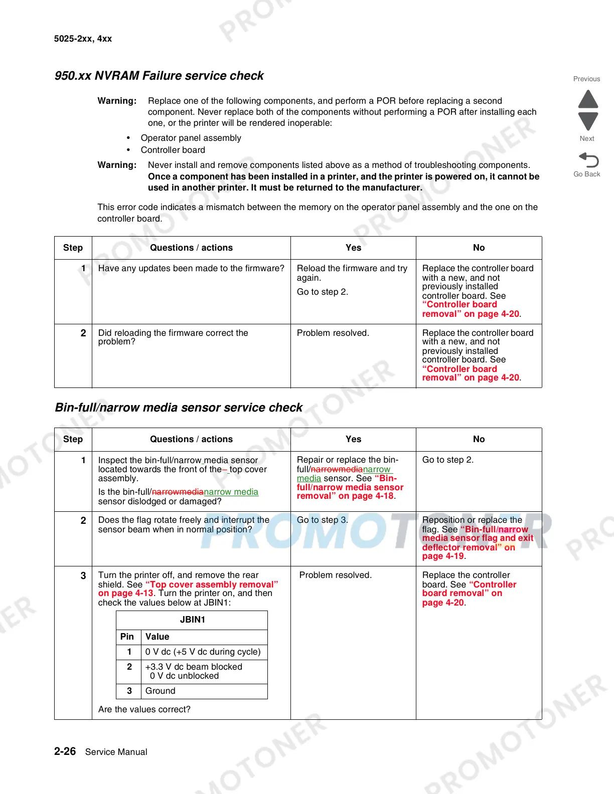
950.xx NVRAM Failure service check
Warning: Replace one of the following components, and perform a POR before replacing a second
component. Never replace both of the components without performing a POR after installing each
one, or the printer will be rendered inoperable:
• Operator panel assembly
• Controller board
Warning: Never install and remove components listed above as a method of troubleshooting components.
Once a component has been installed in a printer, and the printer is powered on, it cannot be
used in another printer. It must be returned to the manufacturer.
This error code indicates a mismatch between the memory on the operator panel assembly and the one on the
controller board.
Bin-full/narrow media sensor service check
Step Questions / actions Yes No
1 Have any updates been made to the firmware? Reload the firmware and try
again.
Go to step 2.
Replace the controller board
with a new, and not
previously installed
controller board. See
“Controller board
removal” on page 4-20.
2
Did reloading the firmware correct the
problem?
Problem resolved. Replace the controller board
with a new, and not
previously installed
controller board. See
“Controller board
removal” on page 4-20.
Step Questions / actions Yes No
1 Inspect the bin-full/narrow
media sensor
located towards the front of the
top cover
assembly.
Is the bin-full/narrowmedia
narrow media
sensor dislodged or damaged?
Repair or replace the bin-
full/narrowmedia
narrow
media sensor. See “Bin-
full/narrow media sensor
removal” on page 4-18.
Go to step 2.
2
Does the flag rotate freely and interrupt the
sensor beam when in normal position?
Go to step 3. Reposition or replace the
flag. See “Bin-full/narrow
media sensor flag and exit
deflector removal” on
page 4-19.
3
Turn the printer off, and remove the rear
shield. See “Top cover assembly removal”
on page 4-13. Turn the printer on, and then
check the values below at JBIN1:
Are the values correct?
Problem resolved. Replace the controller
board. See “Controller
board removal” on
page 4-20.
JBIN1
Pin Value
1 0 V dc (+5 V dc during cycle)
2 +3.3 V dc beam blocked
0 V dc unblocked
3 Ground
 Loading...