3-56 Theory of Operation: Controller
3.2.7 RF Interface
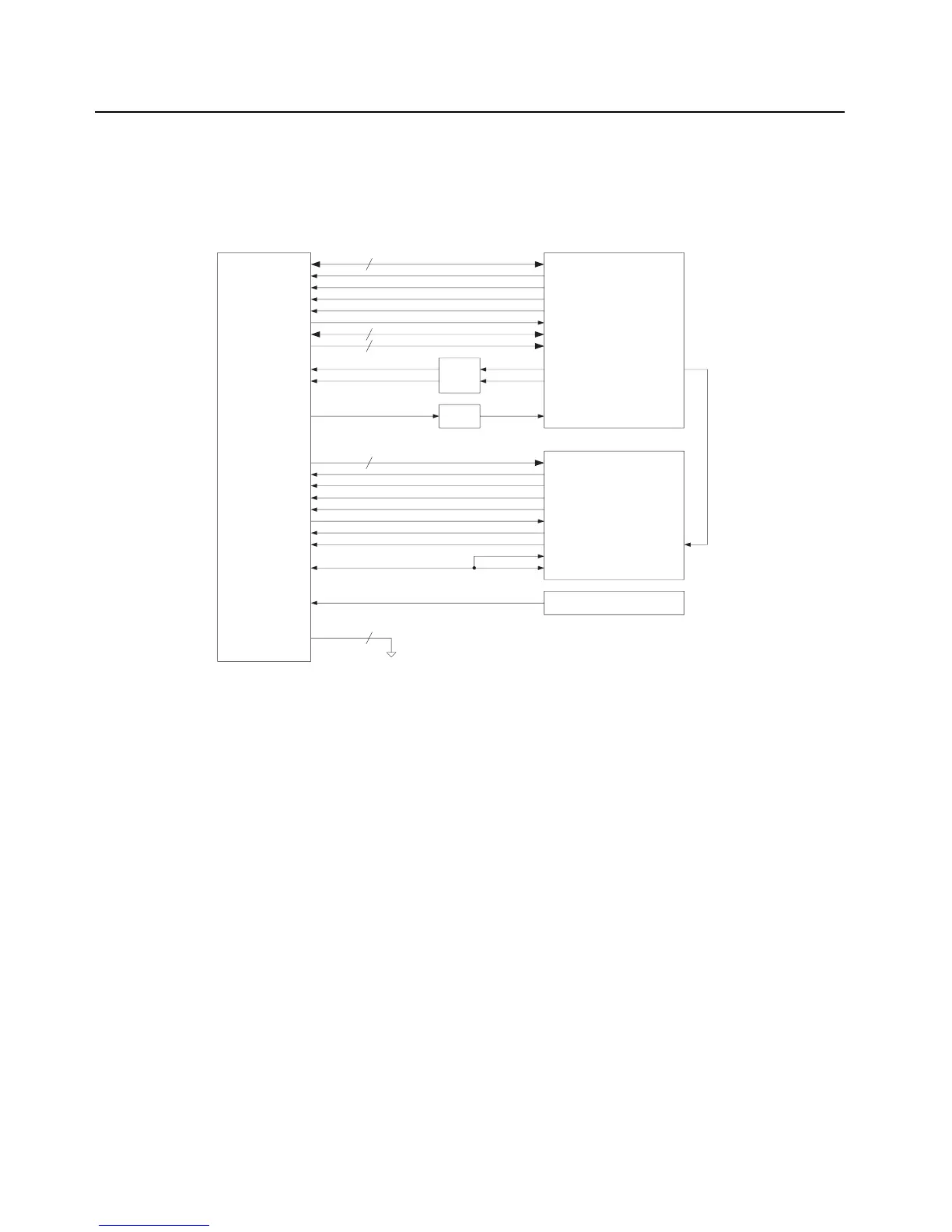
The VOCON to RF board interface through connector J1001. See Figure 3-40.
Figure 3-40. VOCON to RF Board Interface
The major interfaces are the TX and RX SSI buses, the SPI Bus with associated chip selects, the
synchronization signals (DMCS,SYNCB), the 16.8 MHz clock, MAKO VDDs and I/O's, and the
TX Inhibit from the Option Board.
3.2.7.1 TX SSI
The TX SSI interface provides the SSI data from the OMAP's DSP to the Trident IC on the RF board.
The interface contains 3 signals, the TX frame sync, TX clock, and TX Data signals. The pin
numbers for both the RF connector and OMAP IC are also shown in Figure 3-40.
3.2.7.2 RX SSI
The RX SSI interface provides the SSI data from the Abacus IC on the RF board to the OMAP's
DSP. The interface contains 3 signals, the RX frame sync, RX clock, and RX Data signals. The pin
numbers for both the RF connector and OMAP IC are shown in Figure 3-40.
3.2.7.3 Synchronization
The DMCS and SYNCB signals are used for synchronization between the RF and VOCON boards.
These signals route from the OMAP IC timer outputs through the CPLD to the RF board. The DMCS
signal connects to the Trident IC and the SYNCB connects to the ABACUS IC. The pin numbers for
both of the signals are shown in Figure 3-40.
RF - VoCon Interface
OMAP
TX SSI
RX SSI
SPI
ABCS
TRCS
EEPROM_CS
DMCS
SYNCB
LOCK
TEMP
16.8MHz
TUNE
ISET
BATT
VSW1
V2775
GND
BSTAT
TXINH
CPLD
3
3
3
McBSP3
GPIO59
GPIO17
GPIO28
GPIO56
McBSP2
McBSP2
TIMER.PWM2
GPIO7
TIMER.EXTCLKBUFFER
RSTB
5
MAKO
VDD
VSW1
V6
POR
ATOD_5
FE_TUNE1
PWR_CTRL
OPTION BOARD
9
ONE_WIRE_BATT
RF CONNECTOR
LDO2LDO2
GPIO61/SPIF_CS2DAC_CS
L3
V6
G19
T19
V15
M20
Y5
N18
TIMER.PWM1
TX_RX
L14
A1 1
L3
N1
L13
N14,P14,AA1733,31,29
22
27
2
25
14
19,17,21
15,11,13
Y6,W7,AA5
V7,W6,P10
9
23
3
28,30,
32,34,36
37
6
8
7
20
18
16
26
12
1,4,5,10,24,
35,38,39,40
ATOD_4
C1
56
L8
L12
D2
 Loading...