6-3-4.
Connector Pin Configuration & Signal Names
(1) For VS-5E and VS-5ED Models
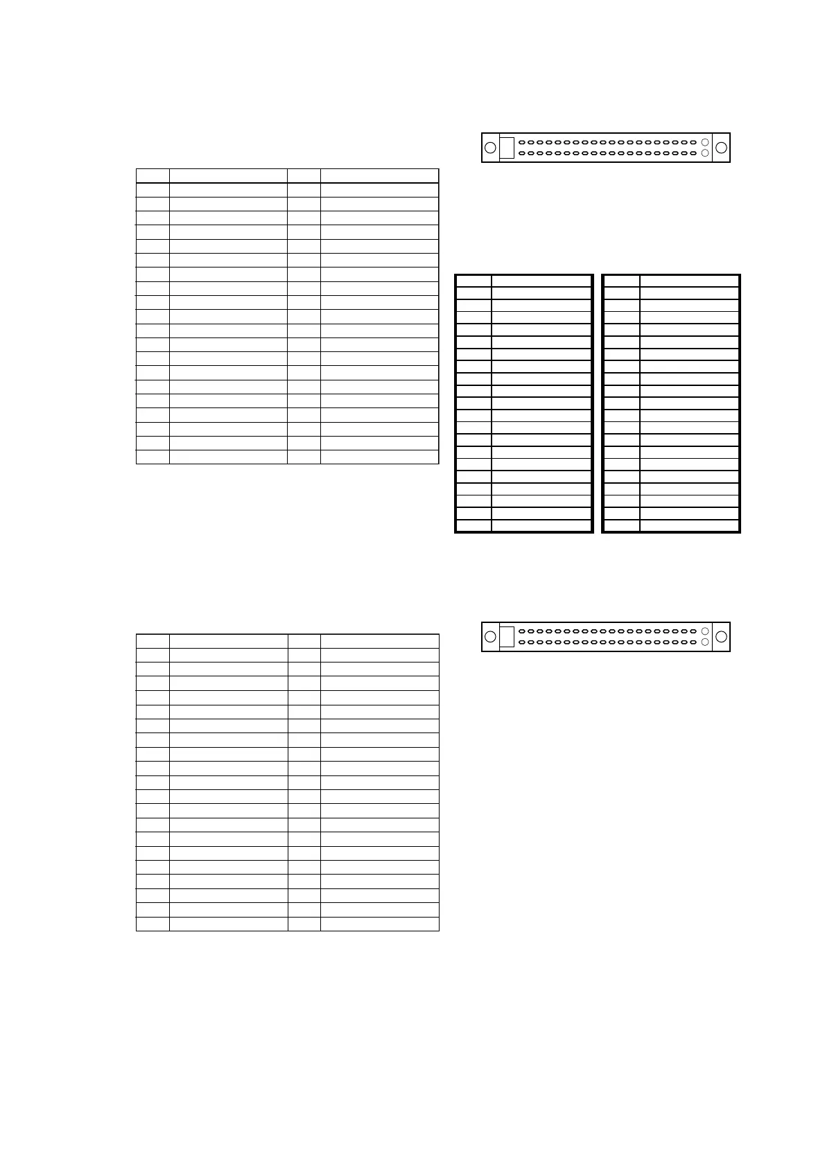
[1] Switch Output Connector (for VS-5E and VS-5ED)
[Connector Model: FCN361J040-AU/FCN-360C040-E] (Fujitsu Co.)
(Connector diagram)
Cable color and marking when external cable is used
[2] BCD Connector (VS-5ED is equipped with this connector)
[Connector Model: FCN361J040-AU/FCN-360C040-E] (Fujitsu Co.)
(Connector diagram)
Pin No. Cable Color & Marking Pin No. Cable Color & Marking
B20 Pink (Black
■■■■
) A20 Pink (Red
■■■■
)
B19 Yellow (Black
■■■■
) A19 Yellow (Red
■■■■
)
B18 White (Black
■■■■
) A18 White (Red
■■■■
)
B17 Gray (Black
■■■■
) A17 Gray (Red
■■■■
)
B16 Orange (Black
■■■■
) A16 Orange (Red
■■■■
)
B15 Pink (Black
■■■
) A15 Pink (Red
■■■
)
B14 Yellow (Black
■■■
) A14 Yellow (Red
■■■
)
B13 White (Black
■■■
) A13 White (Red
■■■
)
B12 Gray (Black
■■■
) A12 Gray (Red
■■■
)
B11 Orange (Black
■■■
) A11 Orange (Red
■■■
)
B10 Pink (Black
■■
) A10 Pink (Red
■■
)
B9 Yellow (Black
■■
) A9 Yellow (Red
■■
)
B8 White (Black
■■
) A8 White (Red
■■
)
B7 Gray (Black
■■
) A7 Gray (Red
■■
)
B6 Orange (Black
■■
) A6 Orange (Red
■■
)
B5 Pink (Black
■
) A5 Pink (Red
■
)
B4 Yellow (Black
■
) A4 Yellow (Red
■
)
B3 White (Black
■
) A3 White (Red
■
)
B2 Gray (Black
■
) A2 Gray (Red
■
)
B1 Orange (Black
■
) A1 Orange (Red
■
)
(External cables can be used at either the switch output
connector or the BCD connector.)
●B-9●
Pin No.
B20
B19
B18
B17
B16
B15
B14
B13
B12
B11
B10
B9
B8
B7
B6
B5
B4
B3
B2
B1
Signal Name
Switch output 1
Switch output 2
Switch output 3
Switch output 4
Switch output 5
Switch output 6
Switch output 7
Switch output 8
Switch output 9
Switch output 10
Switch output 11
Switch output 12
Switch output 13
Switch output 14
Switch output 15
Switch output 16
Pin No.
A20
A19
A18
A17
A16
A15
A14
A13
A12
A11
A10
A9
A8
A7
A6
A5
A4
A3
A2
A1
Signal Name
Switch output 17
Switch output 18
Switch output 19
Switch output 20
Switch output 21
Switch output 22
Switch output 23
Switch output 24
System ready
Timing pulse
0V common
0V common
0V common
0V common
Pin No.
B20
B19
B18
B17
B16
B15
B14
B13
B12
B11
B10
B9
B8
B7
B6
B5
B4
B3
B2
B1
Signal Name
Timing pulse※
Current position HOLD input
Program No.input 1
Program No.input 2
Program No.input 4
24V input common
24V input common
Pin No.
A20
A19
A18
A17
A16
A15
A14
A13
A12
A11
A10
A9
A8
A7
A6
A5
A4
A3
A2
A1
Signal Name
Current position output 0.5
Current position output 1
Current position output 2
Current position output 4
Current position output 8
Current position output 10
Current position output 20
Current position output 40
Current position output 80
Current position output 100
Current position output 200
Latch pulse
Program No.output 1
Program No.output 2
Program No.output 4
0V output common
0V output common
※This output is the same signal at A5.
F
AB
15101520
This drawing shows the arrangement of pins as
viewed from the soldering terminals.
F
AB
15101520
This drawing shows the arrangement of pins as
viewed from the soldering terminals.
Artisan Technology Group - Quality Instrumentation ... Guaranteed | (888) 88-SOURCE | www.artisantg.com
 Loading...