ZCU102 Evaluation Board User Guide www.xilinx.com 29
UG1182 (v1.2) March 20, 2017
Chapter 3: Board Component Descriptions
The ZCU102 DDR4 SODIMM interface adheres to the constraints guidelines documented in
the PCB Guidelines for DDR4 section of UltraScale Architecture PCB Design Guide (UG583)
[Ref 3] The ZCU102 DDR4 SODIMM interface is a 40Ω impedance implementation. Other
memory interface details are also available in the UltraScale Architecture FPGAs Memory
Interface Solutions Guide (PG150) [Ref 4].
DDR4 Component Memory
[Figure 2-1, callout 3]
The 4 Gb, 16-bit wide DDR4 memory system is comprised of one 256 Mb x 16 SDRAM
(Micron MT40A256M16GE-075E) at U2. This memory system is connected to the PL-side
XCZU9EG bank 64. The DDR4 0.6V VTT termination voltage is supplied from sink-source
regulator U35. The connections between the DDR4 memory and XCZU9EG bank 64 are
listed in Table 3-4.
AN28
DDR4_SODIMM_CS0_B 149 CS0_N
AL30
DDR4_SODIMM_CS1_B 157 CS1_N
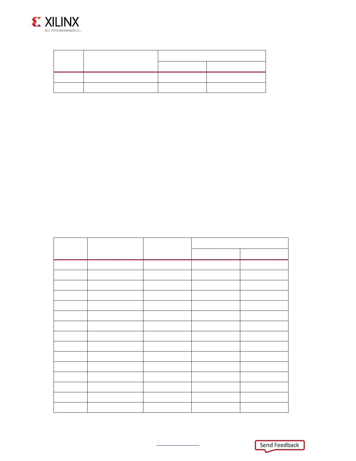
Table 3-4: DDR4 Component Memory Connection to the XCZU9EG MPSoC
XCZU9EG
(U1) Pin
Net Name I/O Standard
DDR4 Component Memory
Pin Number Pin Name
AM8
DDR4_A0 SSTL12_DCI P3 A0
AM9
DDR4_A1 SSTL12_DCI P7 A1
AP8
DDR4_A2 SSTL12_DCI R3 A2
AN8
DDR4_A3 SSTL12_DCI N7 A3
AK10
DDR4_A4 SSTL12_DCI N3 A4
AJ10
DDR4_A5 SSTL12_DCI P8 A5
AP9
DDR4_A6 SSTL12_DCI P2 A6
AN9
DDR4_A7 SSTL12_DCI R8 A7
AP10
DDR4_A8 SSTL12_DCI R2 A8
AP11
DDR4_A9 SSTL12_DCI R7 A9
AM10
DDR4_A10 SSTL12_DCI M3 A10/AP
AL10
DDR4_A11 SSTL12_DCI T2 A11
AM11
DDR4_A12 SSTL12_DCI M7 A12/BC_B
AL11
DDR4_A13 SSTL12_DCI T8 A13
AK12
DDR4_BA0 SSTL12_DCI N2 BA0
Table 3-3: DDR4 SODIMM Socket J1 Connections to FPGA PS DDR Bank 504 (Cont’d)
XCZU9EG
(U1) Pin
Net Name
DDR4 SODIMM Memory J1
Pin Number Pin Name

 Loading...


