ZCU102 Evaluation Board User Guide www.xilinx.com 68
UG1182 (v1.2) March 20, 2017
Chapter 3: Board Component Descriptions
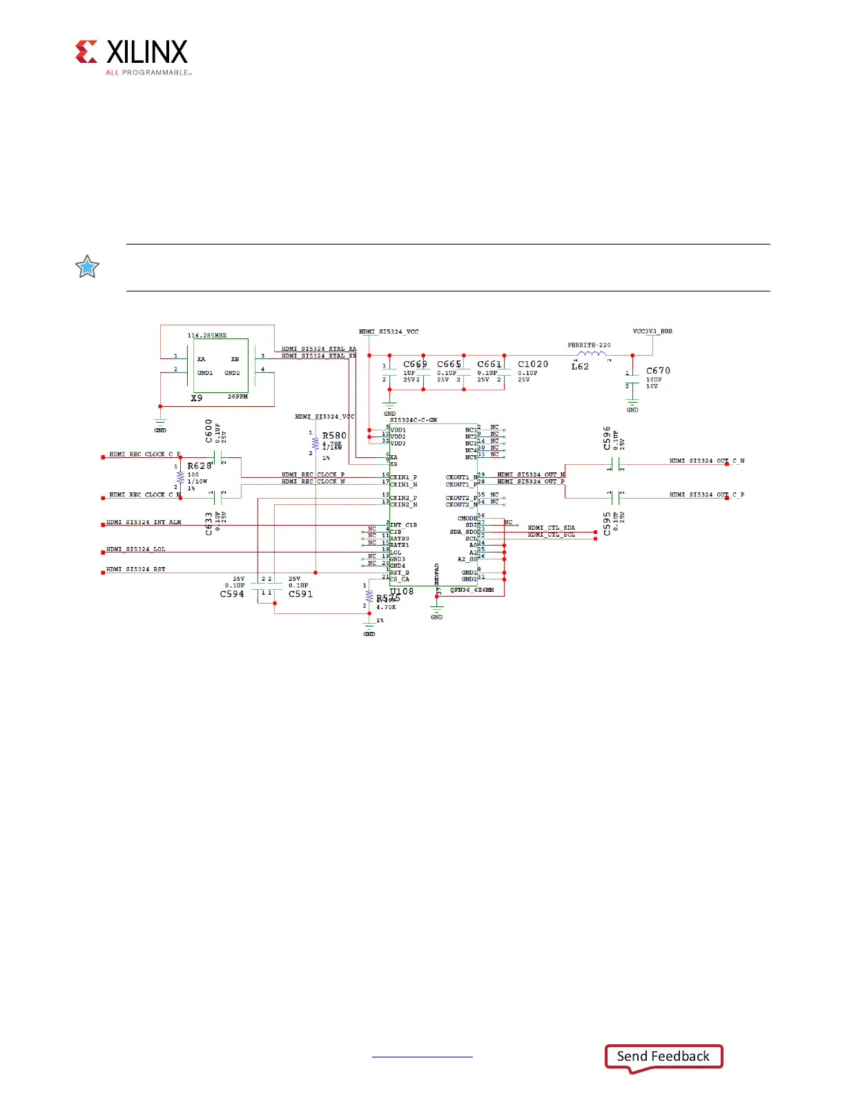
The primary purpose of this clock is to support synchronous protocols (such as CPRI or
OBSAI to perform clock recovery from a user-supplied SFP/SFP+ module) and use the jitter
attenuated recovered clock to drive the reference clock inputs of a GTH transceiver. The
system controller configures the SI5324C in free-run mode (see TI MSP430 System
Controller, page 105). Enabling the jitter attenuation feature requires additional user
programming from the FPGA through the I2C bus. The jitter attenuated clock circuit is
shown in Figure 3-25.
IMPORTANT: The Silicon Labs Si5324C U108 pin 1 reset net HDMI_SI5324_RST must be driven High to
enable the device. U108 pin 1 net HDMI_SI5324_RST is connected to FPGA U1 bank 50 pin J12.
SFP/SFP+ Connector
[Figure 2-1, callout 17]
The ZCU102 board contains a small form-factor pluggable (SFP+) 2x2 quad-connector and
cage assembly that accepts SFP or SFP+ modules. Figure 3-26 shows a typical SFP+ module
connector circuitry implementation. Table 3-30 lists the connections between the
connectors and the XCZU9EG MPSoC.
Note that the SFPx_TX_DISABLE_TRANS default 2-pin jumper strapping is Open which
means the SFPx_TX_DISABLE_TRANS net is pulled High, thus disabling the TX output of SFP
module. The open jumper also allows user-FPGA IP to control activation or deactivation of
SFPx_TX_DISABLE_TRANS on each module independently.
X-Ref Target - Figure 3-25
Figure 3-25: HDMI Interface Clock Recovery

 Loading...


