ZCU102 Evaluation Board User Guide www.xilinx.com 64
UG1182 (v1.2) March 20, 2017
Chapter 3: Board Component Descriptions
PCIe Reset (MIO 31)
The Zynq UltraScale+ MPSoC contains an integrated block for PCI Express interface based
on the PCIe base v2.1 specification. The PS-side PCIe reset signal is wired to the PCIe
Gen2 x4 root port slot P1. The MIO31 pin is an output for PCIe Root Port mode operation on
the ZCU102.
PMU GPO (MIO 32-37)
The platform management unit (PMU) within the Zynq UltraScale+ MPSoC signals power
domain changes using the PMU output pins for deep-sleep mode. The Zynq UltraScale+
MPSoC PMU GPO pins are connected to inputs of the MSP430 system controller via
TXS0108E level-shifter U141. The connections from MPSoC U1 Bank 501 to MSP430 U41 are
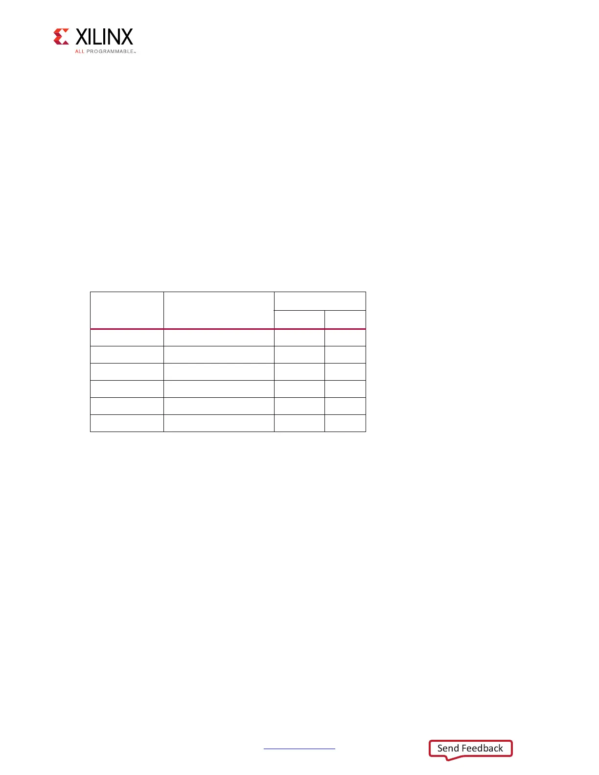
listed in Table 3-28.
Through the I2C0 Bus MPSoC MIO pins, the PMU has access to the board power controllers
and power monitors. See Figure 3-17, page 55 for more details.
Refer the Zynq UltraScale+ MPSoC Technical Reference Manual (UG1085) [Ref 2] for more
details about the PMU interface.
HDMI Video Output
[Figure 2-1, callout 14]
The ZCU102 board provides a high-definition multimedia interface (HDMI®) video output
using a TI SN65DP159RGZ HDMI re-timer at U94. The HDMI output is provided on a TE
Connectivity 1888811-1 right-angle dual-stacked HDMI type-A receptacle at P7. The
SN65DP159RGZ device is a dual mode DisplayPort to transition-minimized differential
signal (TMDS) re-timer supporting digital video interface (DVI) 1.0 and high-definition
multimedia interface (HDMI) 1.4b and 2.0 output signals. The SN65DP159RGZ device
supports the dual mode standard version 1.1 type 1 and type 2 through the DDC link or AUX
channel. The SN65DP159RGZ device supports data rates up to 6 Gb/s per data lane to
support Ultra HD (4K x 2K / 60 Hz) 8-bits per color high-resolution video and HDTV with
Table 3-28: XCZU9EG U1 to MSP430 Connections
XCZU9EG (U1)
Pin
Schematic Net Name
MSP430 U41
Pin Name Pin No.
N22
MIO37_PMU_GPO5
P1_0 13
K23
MIO36_PMU_GPO4
P1_1 14
P22
MIO35_PMU_GPO3
P1_2 15
L22
MIO34_PMU_GPO2
P1_3 16
H23
MIO33_PMU_GPO1
P1_4 17
H22
MIO32_PMU_GPO0
P1_5 18

 Loading...


