ZCU102 Evaluation Board User Guide www.xilinx.com 93
UG1182 (v1.2) March 20, 2017
Chapter 3: Board Component Descriptions
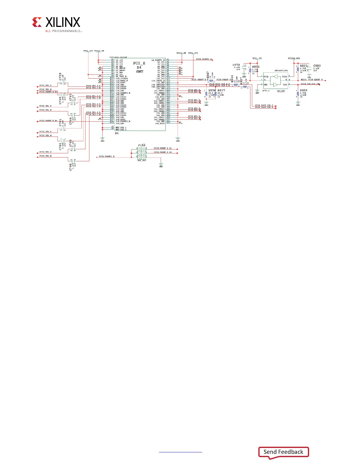
The 4-lane PCIe connector lane TX/RX nets are wired to the MPSoC U1 PS GTR Bank 505
transceiver channels through four 2-to-1 Pericom PI2DBS6212 [Ref 20] high speed
multiplexers.
FPGA Mezzanine Card Interface
[Figure 2-1, callouts 31, 32]
The ZCU102 evaluation board supports the VITA 57.1 FPGA mezzanine card (FMC)
specification [Ref 22] by providing subset implementations of high pin count connectors at
J5 (HPC0) and J4 (HPC1). HPC connectors use a 10 x 40 form factor, populated with 400 pins.
The connectors are keyed so that a mezzanine card, when installed in either of these FMC
connectors on the ZCU102 evaluation board, faces away from the board.
FMC HPC0 Connector J5
[Figure 2-1, callout 31]
The FMC connector at J5 (HPC0) implements a subset of the full FMC HPC connectivity:
• 68 single-ended, or 34 differential user-defined pairs (34 LA pairs: LA[00:33])
• Eight GTH transceiver DP differential pairs
• Two GBTCLK differential clocks
• 159 ground and 15 power connections
X-Ref Target - Figure 3-38
Figure 3-38: PCIe Connector P1

 Loading...


