REV.-A
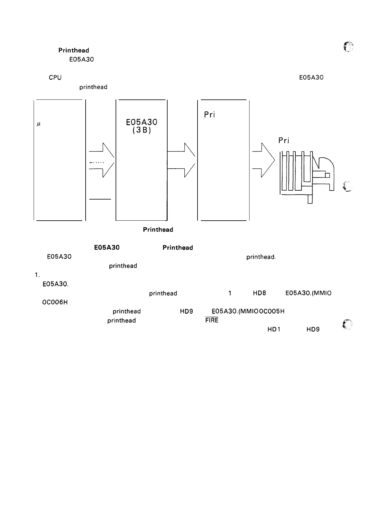
2.2.5.3 Printhead Drive Circuit Block Diagram
Gate array
E05A30
is used as an 8-bit + l-bit data latch.
The
CPU determines the pulse width for the head-wire drive pulses from gate array
E05A30
by
monitoring the
printhead
drive power (+24 V line).
CPU
~
PD78 10HG
(2C)
--N
DATA
--l/
FIRE
●
GA
E05A30
(3B)
I
Pri
nthead
D rive
C i rc u it
Pri
ntherd
3
.
.
.
.
.
.
‘i_
1.
2.
3.
4.
Figure 2-43. Printhead Drive Circuit Block Diagram
2.2.5.4 Gate Array
E05A30
Operation in Printhead Drive Circuit
The
E05A30
gate array includes circuitry to interface the CPU and the printhead.
The data is output to the
printhead in the following sequence:
Print data is expanded in the image buffer as dot patterns. The CPU outputs the dot patterns to the
E05A30.
The data for pins 1 through 8 of the printhead is latched by HD
1
trough HD8 of the
E05A30.
(MMIO
OCO06H write operation)
The data for pin 9 of the
printhead is latched by HD9 of the
E05A30.
(MMIO
OCO05H write operation)
After data latching, the
printhead drive pulse width signal
~
is output from the CPU’s event counter.
When the signal is LOW, the gate array will be open, so that the data from
HD1 through HD9 will
be output.
2-40
 Loading...