Appendix A
-
134
-
A.5.2 Multifunctional PG Card (MD38PGMD)
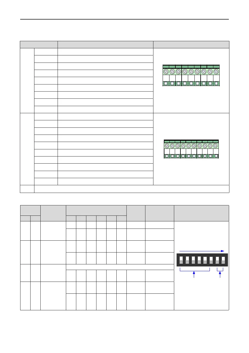
Table A-8 Terminal descriptions of MD38PGMD
Terminal Function Description Terminal Arrangement
CN2
A+ Encoder output signal A positive
J3
A+ A- B+ B- Z+ Z- COM PE
5/15
A- Encoder output signal A negative
B+ Encoder output signal B positive
B- Encoder output signal B negative
Z+ Encoder output signal Z positive
Z- Encoder output signal Z negative
5V/15V Encoder 5V/15V power supply
COM Encoder power ground
PE Shield connecting point
J7
OA+ Differential frequency dividing output signal A positive
OA+
OA- OB+
OB-
OZ+ OZ-
OA OB
GND
OZ
OA- Differential frequency dividing output signal A negative
OB+ Differential frequency dividing output signal B positive
OB- Differential frequency dividing output signal B negative
OZ+ Differential frequency dividing output signal Z positive
OZ- Differential frequency dividing output signal Z negative
GND Frequency dividing output reference ground
OA Open-collector frequency dividing output signal A
OB Open-collector frequency dividing output signal B
OZ Open-collector frequency dividing output signal Z
CN1 18-pin FFC interface, connecting to J4 on the control board of the AC drive
Table A-9 Descriptions of DIP Switch of MD38PGMD
Filter
Selection
Denition
Address Setting
Value
Frequency
Dividing
Coefcient
DIP Switch
8 7 6 5 4 3 2 1
0 0
Non-self-
adaptive
lter
0 0 0 0 0 0 Reserved No output
Filter
selection
Frequency dividing
coefficient setting
ON
1
2
3
4
5
6
7
8
DIP
Low bit
High bit
0 0 0 0 0 1 1
Frequency
divided by 1
0 1
Self-adaptive
lter
0 0 0 0 1 0 2
Frequency
divided by 2
0 0 0 0 1 1 3
Frequency
divided by 3
1 0
Fixed inter-
lock
...
1 1 1 1 0 1 61
Frequency
divided by 61
1 1
Automatic
inter-
lock
1 1 1 1 1 0 62
Frequency
divided by 62
1 1 1 1 1 1 63
Frequency
divided by
63
 Loading...