Bus Operation
7-38 MC68030 USER’S MANUAL MOTOROLA
7.3.2 Asynchronous Write Cycle
During a write cycle, the processor transfers data to memory or a peripheral device.
Figure 7-24 is a flowchart of a write cycle operation for a long-word transfer. The following
figures show the functional write cycle timing diagrams specified in terms of clock periods.
Figure 7-25 shows two write cycles (between two read cycles with no idle time) for a 32-bit
port. Figure 7-26 shows byte and word write cycles to a 32-bit port. Figure 7-27 shows a
long-word write cycle to an 8-bit port. Figure 7-28 shows a long-word write cycle to a 16-bit
port.
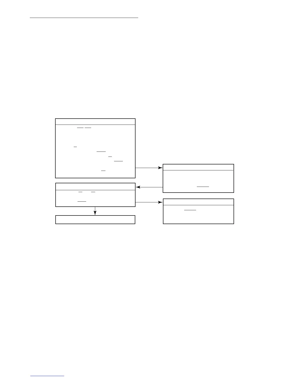
Figure 7-24. Asynchronous Write Cycle Flowchart
1) ASSERT ECS/OCS FOR ONE-HALF CLOCK
2) DRIVE ADDRESS ON A31-A0
3) DRIVE FUNCTION CODE ON FC2-FC0
4) DRIVE SIZE (SIZ1-SIZ0) (FOUR BYTES)
5) SET R/W TO WRITE
6) CACHE INHIBIT OUT (CIOUT) BECOMES VALID
7) ASSERT ADDRESS STROBE (AS)
8) ASSERT DATA BUFFER ENABLE (DBEN)
9) DRIVE DATA LINES D31-D0
10) ASSERT DATA STROBE (DS)
1) NEGATE AS AND DS
2) REMOVE DATA FROM D31-D0
3) NEGATE DBEN
EXTERNAL DEVICECONTROLLER
1) NEGATE DSACKx
TERMINATE CYCLE
ACCEPT DATA
1) DECODE ADDRSS
2) STORE DATA FROM D31-D0
3) ASSERT DATA TRANSFER AND SIZE
ACKNOWLEDGE (DSACKx)
ADDRESS DEVICE
TERMINATE OUTPUT TRANSFER
START NEXT CYCLE

 Loading...