G147 6-28 SM
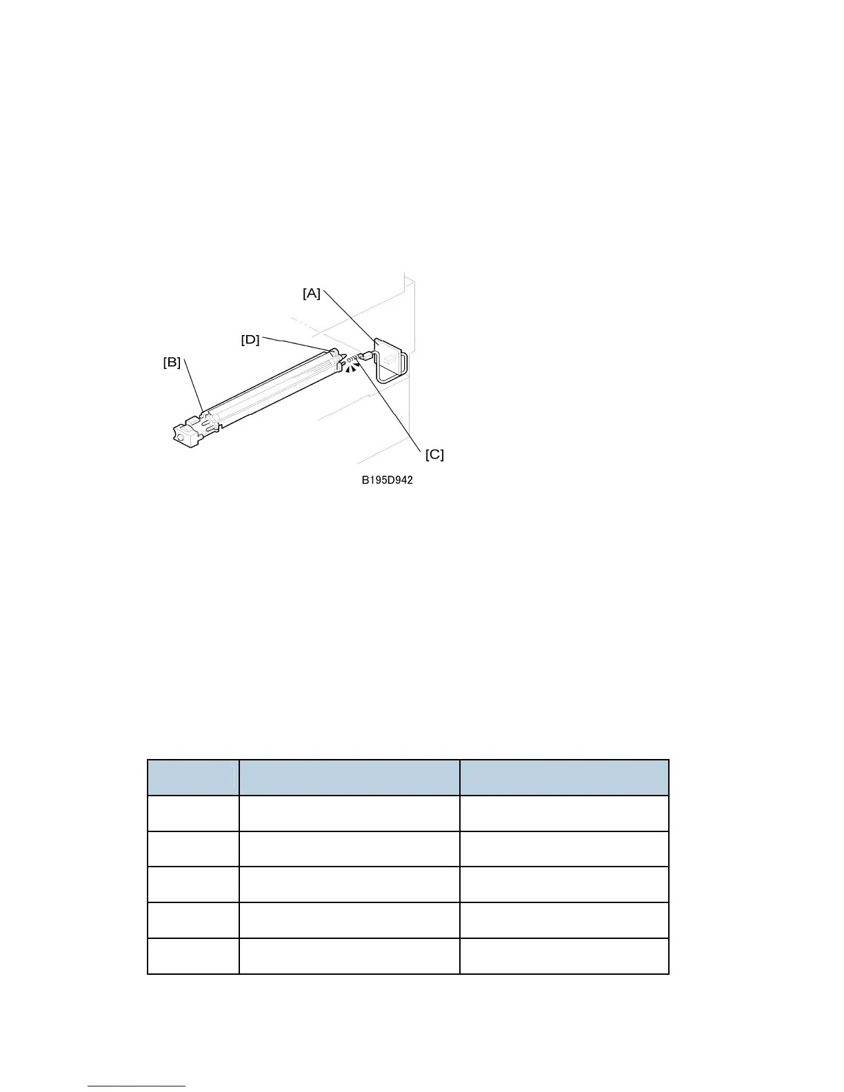
unit at [D].
6.7.4 DEVELOPMENT BIAS
Development Bias Mechanism
Black areas of the latent image are at a low negative charge (about 150 V) and white areas
are at a high negative charge (about –950 V).
To attract negatively charged toner to the black areas of the latent image on the drum, the
high voltage supply board [A] applies a bias of –540 volts to the development roller
throughout the image development process. The bias is applied to the development roller
shaft [B] through the bias terminal spring [C] and bias terminal [D].
The development bias voltage (–540 V) can be adjusted with SP2201 (Development Bias).
Correction for Paper Width and Thickness (By-pass Tray only)
The by-pass tray can be used for non-standard paper narrow than sizes accepted by the
paper trays. Thicker paper, OHP sheets, etc. can also be loaded in the by-pass tray but
adjustments must be performed with the SP modes listed below in order to avoid jams and
misfeeds.
SP Mode SP Name
SP2201-01 Developer Bias – Image Dev. Bias Default: -540 V
SP2309-01 Paper Lower Width [a] Width limit. Default: 150 mm
SP2309-02 Paper Upper Width [b] Width limit. Default: 216 mm
SP2914-03 Process Ctrl Set – B gamma Adjust 10 V/step. Default 200 V
SP2914-04 Process Ctrl Set – B delta Adjust 10 V/step. Default 50 V
 Loading...