Circuit Description—
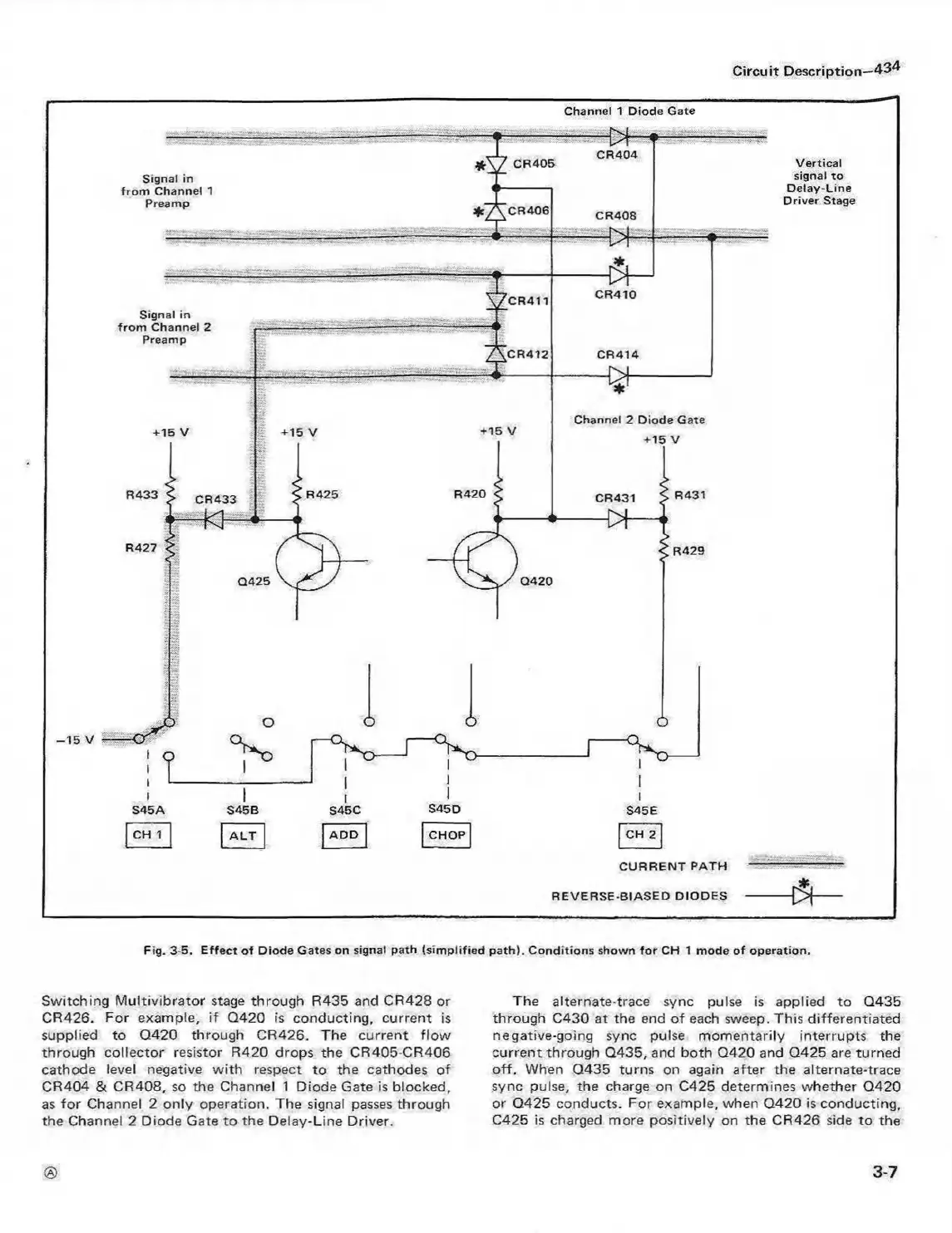
Channel 1 Diode Gate
C U R R E N T P ATH
REVE R S E-BIA S ED D IO DES
Vertica l
signal to
Delay-Line
Driver Stage
Fig. 3-5. E ffe ct o f Diode Gates on signal path (sim plifie d pa th). C o nditions shown fo r CH 1 mode o f operation.
Switching M ultivibrator stage through R435 and CR428 or
CR426. For example, if Q420 is conducting, current is
supplied to Q420 through CR426. The current flow
through collector resistor R420 drops the CR405-CR406
cathode level negative with respect to the cathodes of
CR404 & CR408, so the Channel 1 Diode Gate is blocked,
as fo r Channel 2 only operation. The signal passes through
the Channel 2 Diode Gate to the Delay-Line Driver.
The alternate-trace sync pulse is applied to Q435
through C430 at the end of each sweep. This differentiated
negative-going sync pulse momentarily interrupts the
current through Q435, and both Q420 and Q425 are turned
off. When Q435 turns on again after the alternate-trace
sync pulse, the charge on C425 determines whether Q420
or Q425 conducts. For example, when Q420 is conducting,
C425 is charged more positively on the CR426 side to the
3-7
 Loading...


