7 Series FPGAs GTP Transceivers User Guide www.xilinx.com 75
UG482 (v1.9) December 19, 2016
Chapter 3
Transmitter
TX Overview
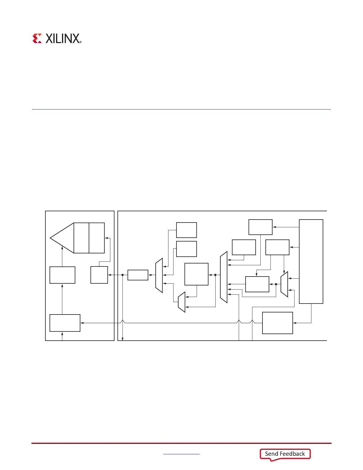
Functional Description
This chapter shows how to configure and use each of the functional blocks inside the transmitter
(TX). Each transceiver includes an independent transmitter, which consists of a PCS and a PMA.
Figure 3-1 shows the functional blocks of the transmitter. Parallel data flows from the FPGA logic
into the FPGA TX interface, through the PCS and PMA, and then out the TX driver as high-speed
serial data.
The key elements within the GTP transceiver TX are:
1. FPGA TX Interface, page 76
2. TX 8B/10B Encoder, page 83
3. TX Gearbox, page 86
4. TX Buffer, page 93
X-Ref Target - Figure 3-1
Figure 3-1: GTP Transceiver TX Block Diagram
TX PMA TX PCS
FPGA
TX
Interface
TX
Gearbox
UG482_c3_01_11281
TX PIPE
Control
Phase
Adjust
FIFO
PCIe
Beacon
From RX Parallel Data
(Far-End PMA Loopback)
To RX Parallel Data
(Near-End PCS Loopback)
Clock from PLL0 or PLL1
From RX Parallel Data
(Far-End PCS Loopback)
PISO
TX
Pre/
Post
Emp
TX Clock
Dividers
TX Phase
Interpolator
TX Phase
Interpolator
Controller
TX
OOB
and
PCIe
TX
Driver
Polarity
SATA
OOB
8B/10B
Encoder
Pattern
Generator
 Loading...