7 Series FPGAs GTP Transceivers User Guide www.xilinx.com 217
UG482 (v1.9) December 19, 2016
Chapter 5
Board Design Guidelines
Overview
Topics related to implementing a design on a printed circuit board using the 7 series Artix™-7
FPGA GTP transceivers are presented in this chapter. The GTP transceivers are analog circuits that
require special consideration and attention when designing and implementing them on a printed
circuit board. Besides an understanding of the functionality of the device pins, a design that
performs optimally requires attention to issues such as device interfacing, transmission line
impedance and routing, power supply design filtering and distribution, component selection, and
PCB layout and stackup design.
Pin Description and Design Guidelines
GTP Pin Descriptions
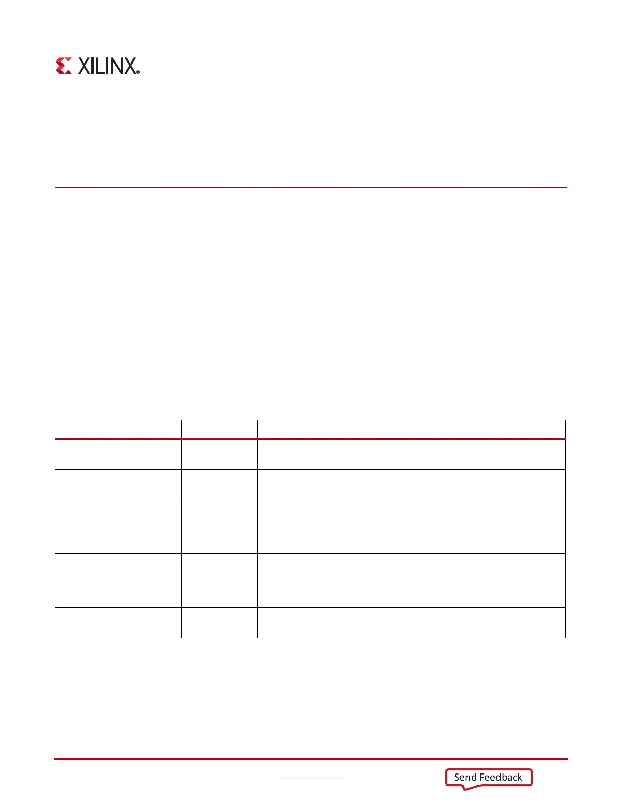
Table 5-1: GTP Quad Pin Descriptions
Pins Direction Description
MGTREFCLK0P
MGTREFCLK0
In (Pad) Differential clock input pin pair for the reference clock of the GTP transceiver
Quad.
MGTREFCLK1P
MGTREFCLK1N
In (Pad) Differential clock input pin pair for the reference clock of the GTP transceiver
Quad.
MGTPRXP0/MGTPRXN0
MGTPRXP1/MGTPRXN1
MGTPRXP2/MGTPRXN2
MGTPRXP3/MGTPRXN3
In (Pad) RXP and RXN are the differential input pairs for each of the receivers in the
GTP transceiver Quad.
MGTTXP0/MGTPTXN0
MGTTXP1/MGTPTXN1
MGTTXP2/MGTPTXN2
MGTTXP3/MGTPTXN3
Out (Pad) TXP and TXN are the differential output pairs for each of the transmitters in
the GTP transceiver Quad.
MGTRREF In (Pad) Calibration resistor input pin for the termination resistor calibration circuit.
Connect to a 100Ω resistor that is also connected to MGTAVTT.
 Loading...