7 Series FPGAs GTP Transceivers User Guide www.xilinx.com 141
UG482 (v1.9) December 19, 2016
RX CDR
RX CDR
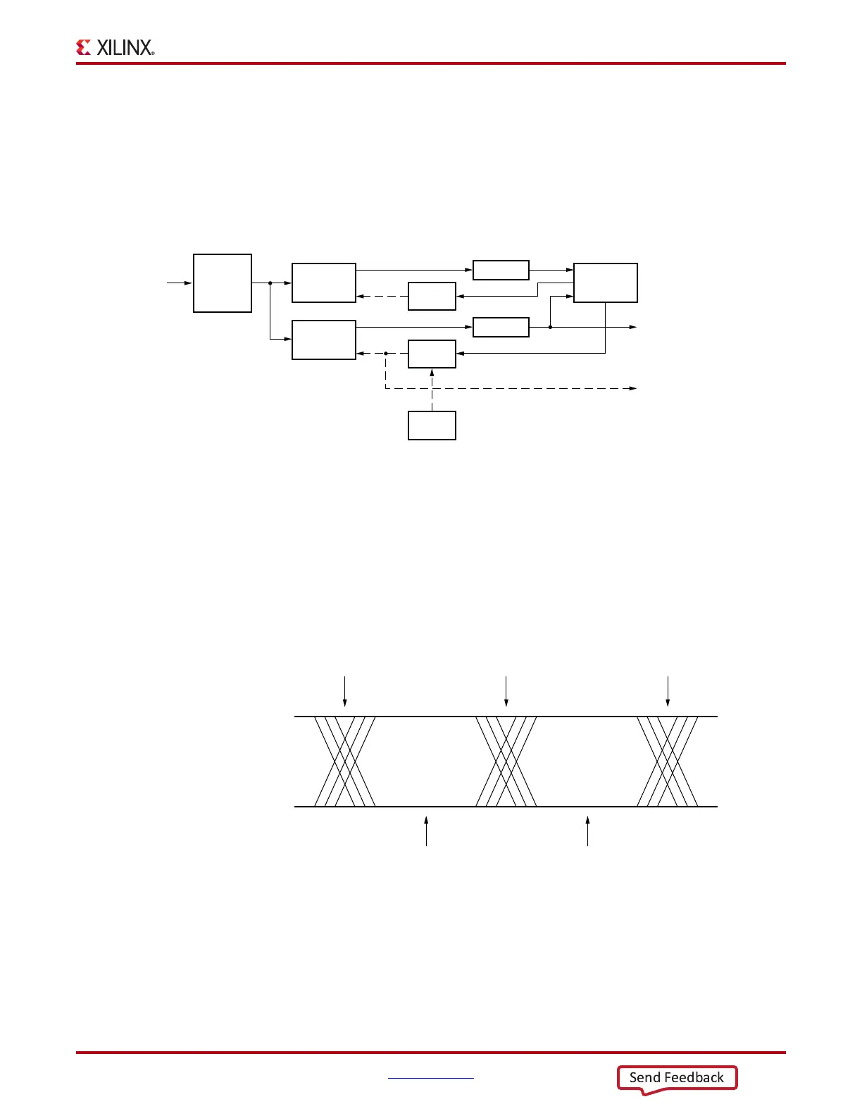
Functional Description
The RX clock data recovery (CDR) circuit in each GTPE2_CHANNEL transceiver extracts the
recovered clock and data from an incoming data stream. Figure 4-16 illustrates the architecture of
the CDR block. Clock paths are shown with dotted lines for clarity.
The GTPE2_CHANNEL transceiver employs phase rotator CDR architecture. Incoming data first
goes through receiver equalization stages. The equalized data is captured by an edge and a data
sampler. The data captured by the data sampler is fed to the CDR state machine and the downstream
transceiver blocks.
The CDR state machine uses the data from both the edge and data samplers to determine the phase
of the incoming data stream and to control the phase interpolators (PIs). The phase for the edge
sampler is locked to the transition region of the data stream while the phase of the data sampler is
positioned in the middle of the data eye.
The PLL0 or PLL1 provides a base clock to the phase interpolator. The phase interpolator in turn
produces fine, evenly spaced sampling phases to allow the CDR state machine to have fine phase
control. The CDR state machine can track incoming data streams that can have a frequency offset
from the local PLL reference clock.
X-Ref Target - Figure 4-16
Figure 4-16: CDR Detail
Linear EQ
CDR FSM
DEMUX
DEMUX
Edge
Sampler
Data
Sampler
PI(X)
PI(D)
RX DATA
Recovered Clock
RXP/N
UG482_c4_06_110911
PLL
X-Ref Target - Figure 4-17
Figure 4-17: CDR Sampler Positions
E
0
E
1
UG482_c4_07_110911
E
2
D
0
D
1
 Loading...