226 www.xilinx.com 7 Series FPGAs GTP Transceivers User Guide
UG482 (v1.9) December 19, 2016
Chapter 5: Board Design Guidelines
Notes relative to Figure 5-7:
1. Nominal values. Refer to DS181
, Artix-7 FPGAs Data Sheet: DC and Switching
Characteristics for values and tolerances.
GTP Reference Clock Checklist
The following criteria must be met when choosing an oscillator for a design with GTP transceivers:
• Provide AC coupling between the oscillator output pins and the dedicated GTP Quad clock
input pins.
• Ensure that the differential voltage swing of the reference clock is the range as specified in
DS181
, (the nominal range is 350 mV – 2,000 mV, and the nominal typical value is
1,200 mV).
• Meet or exceed the reference clock characteristics as specified in DS181
.
• Meet or exceed the reference clock characteristics as specified in the standard for which the
GTP transceiver provides physical layer support.
• Fulfill the oscillator vendor's requirement regarding power supply, board layout, and noise
specification.
• Provide a dedicated point-to-point connection between the oscillator and GTP Quad clock
input pins.
• Keep impedance discontinuities on the differential transmission lines to a minimum
(impedance discontinuities generate jitter).
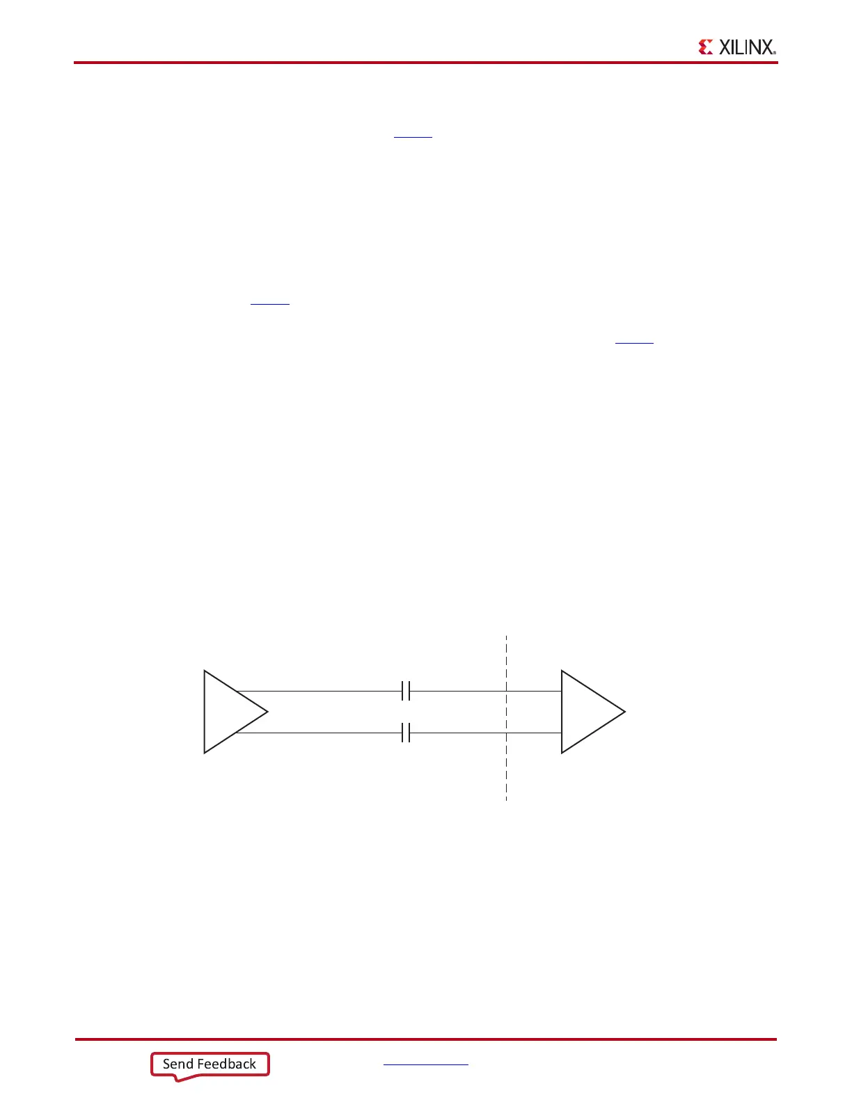
Reference Clock Interface
LVDS
See Figure 5-8.
X-Ref Target - Figure 5-8
Figure 5-8: Interfacing LVDS Oscillator to Artix-7 FPGA GTP Reference Clock Input
0.1µF
LVDS Oscillator
0.1µF
Internal to Artix-7 FPGA
GTP Reference Clock
Input Buffer
UG482_c5_08_080612
 Loading...