7 Series FPGAs GTP Transceivers User Guide www.xilinx.com 225
UG482 (v1.9) December 19, 2016
Reference Clock
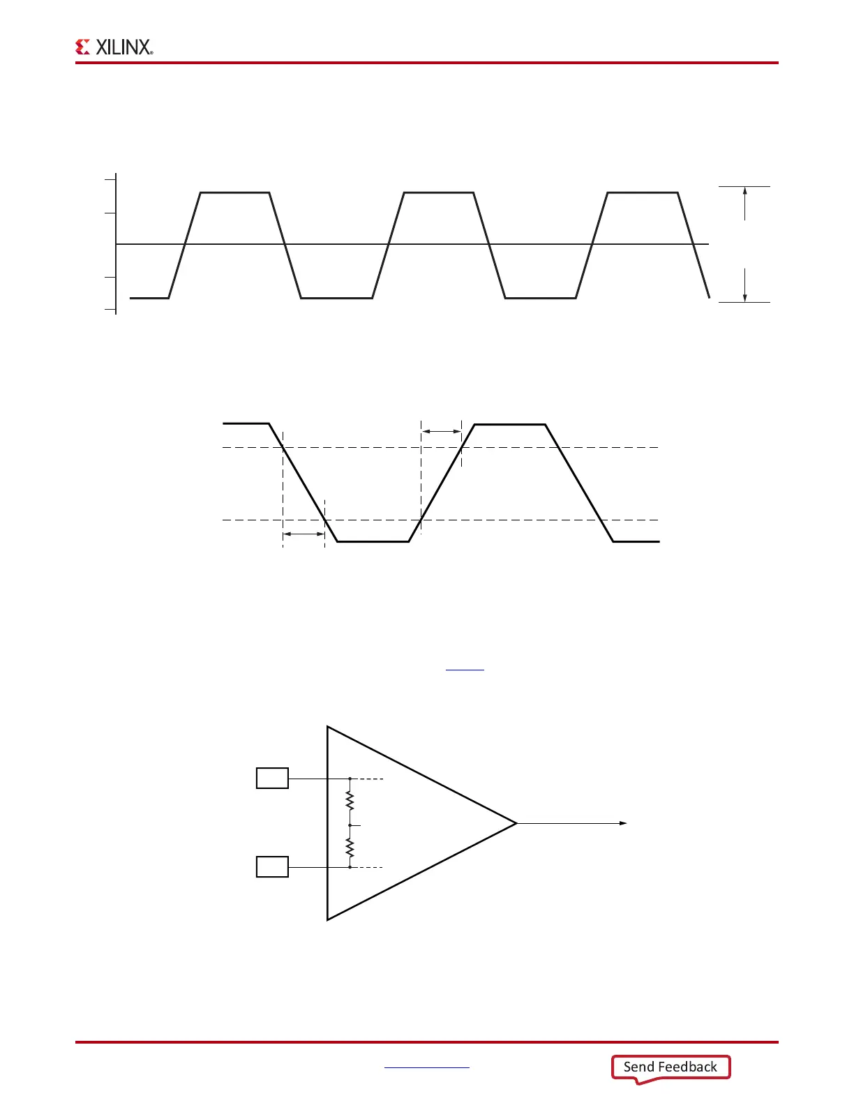
Figure 5-5 illustrates the differential clock input voltage swing, peak-to-peak, which is defined as
MGTREFCLKP - MGTREFCLKN and used in the GTP transceiver portion of the Artix-7 FPGA
data sheet.
Figure 5-6 shows the rise and fall time convention of the reference clock.
Figure 5-7 illustrates the internal details of the IBUFDS. The dedicated differential reference clock
input pair MGTREFCLKP/MGTREFCLKN is internally terminated with 100Ω differential
impedance. The common mode voltage of this differential reference clock input pair is 4/5 of
MGTAVCC, or nominal 0.8V. Refer to DS181
, Artix-7 FPGAs Data Sheet: DC and Switching
Characteristics for exact specifications.
X-Ref Target - Figure 5-5
Figure 5-5: Differential Clock Input Voltage Swing, Peak-to-Peak
MGTREFCLKP - MGTREFCLKN
V
IDIFF
UG482_c5_05_072412
+V
0
–V
X-Ref Target - Figure 5-6
Figure 5-6: Rise and Fall Time
T
RCLK
T
FCLK
80%
20%
UG482_c5_06_080612
X-Ref Target - Figure 5-7
Figure 5-7: MGTREFCLK Input Buffer Details
UG482_c5_07_080612
REFCLK
To GTP
Dedicated
Clock
Routing
MGTREFCLKP
MGTREFCLKN
4/5 MGTAVCC
50
(1)
Ω
50
(1)
Ω
 Loading...