7 Series FPGAs GTP Transceivers User Guide www.xilinx.com 227
UG482 (v1.9) December 19, 2016
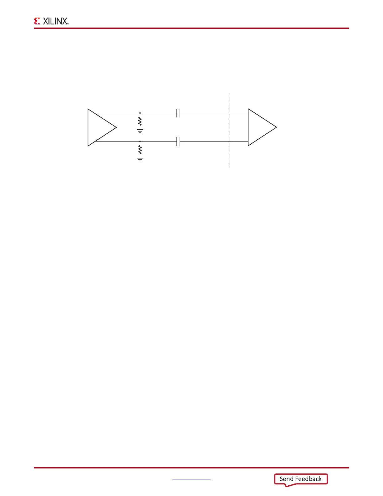
Reference Clock
LVPECL
See Figure 5-9.
Notes relative to Figure 5-9:
1. Nominal values. Refer to the oscillator vendor data sheet for actual bias resistor requirement.
AC Coupled Reference Clock
AC coupling of the oscillator reference clock output to the GTP Quad reference clock inputs serves
multiple purposes:
• Blocking a DC current between the oscillator and the GTP Quad dedicated clock input pins
(which reduces the power consumption of both parts as well).
• Common mode voltage independence.
• The AC coupling capacitor forms a high-pass filter with the on-chip termination that attenuates
a wander of the reference clock.
To minimize noise and power consumption, external AC coupling capacitors between the sourcing
oscillator and the GTP Quad dedicated clock reference clock input pins are required.
Unused Reference Clocks
It is recommended to leave the unused differential input pin clock pair floating (both
MGTREFCLKP and MGTREFCLKN).
Reference Clock Power
The GTP reference clock input circuit is powered by MGTAVCC. Excessive noise on this supply
will have a negative impact on the performance of any GTP Quad that uses the reference clock from
this circuit.
X-Ref Target - Figure 5-9
Figure 5-9: Interfacing LVPECL Oscillator to Artix-7 FPGA GTP Reference Clock Input
0.1µF
0.1µF
Internal to Artix-7 FPGA
GTP Reference Clock
Input Buffer
UG482_c5_09_080612
240
(1)
LVPECL
Oscillator
Ω
240
(1)
Ω
 Loading...