
Do you have a question about the Intel 386 and is the answer not in the manual?
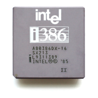
| Architecture | x86 |
|---|---|
| Clock Speed | 12 MHz to 40 MHz |
| Transistor Count | 275, 000 |
| Data Bus Width | 32-bit |
| Address Bus Width | 32-bit |
| Instruction Set | x86 |
| Introduced | 1985 |
| Maximum Memory | 4 GB |
| Operating Modes | Real mode, Protected mode, Virtual 8086 mode |
| MMU | Yes |
| Voltage | 5V |
| Model | Intel 386 |
| Package | PGA |
| Process | 1.5 μm to 1 μm |
Summarizes the contents of the remaining chapters and appendixes, covers notational conventions and special terminology.
Describes the device features and potential applications of the Intel386 EX processor.
Describes the differences between the Intel386 EX processor core and the Intel386 SX processor core.
Describes system registers, I/O address space, address decoding, and addressing modes.
Explains how to configure the device for various applications, including peripheral and pin configurations.
Describes bus interface logic, bus states, bus cycles, and instruction pipelining.
Describes Intel’s System Management Mode (SMM), its hardware interface, and programming.
Describes clock generation circuitry, power management modes, and system reset logic.
Explains symbols, variable formats, instruction mnemonics, numbers, and units of measure.
Defines terms like Assert/Deassert, DOS I/O Address, Expanded I/O Address, PC/AT Address, Processor and CPU.
Lists documents containing additional information for designing systems with the Intel386 EX processor.
Details Intel's FaxBack service, application BBS, CompuServe forums, and World Wide Web for technical information.
Provides contact information for technical support representatives and local distributors for assistance.
Lists Intel literature centers for ordering product literature.
Describes the modular, fully static Intel386 CX central processing unit (CPU) and its enhancements.
Details PC-compatible and embedded application-specific peripherals integrated into the Intel386 EX processor.
Details System Management Mode and additional address lines introduced in the Intel386 CX processor core.
Describes the internal architecture of the Intel386 CX processor, including its functional units and pipelining.
Explains the connection of Intel386 EX processor peripherals to the core via the internal Bus Interface Unit (BIU).
Categorizes Intel386 EX processor register resources into core architecture and peripheral registers.
Describes the 64 Kbyte I/O address space used by PC/AT platforms and how it's mapped.
Details the I/O address scheme similar to EISA/E-ISA, repeated within the 64 Kbyte range.
Lists the physical locations of integrated peripheral registers, primarily in slot 15 of the I/O space.
Explains configurable I/O address mapping, DOS I/O space, and the REMAPCFG register.
Describes four peripheral addressing modes derived from ESE bit and REMAPCFG remap bits.
Lists addresses and names of user-accessible peripheral registers, including reset values.
Explains device configuration as setting up microprocessor peripherals for a system design.
Describes configuration for DMA, Interrupt Control, Timer/Counter, SIO, SSIO, Chip-select, and Watchdog Timer units.
Details signal pairs on pins without multiplexers and pin configuration registers.
Outlines a procedure for configuring the microprocessor, including pin, peripheral, and review steps.
Presents a PC/AT-compatible configuration example with design requirements and solutions.
Describes the external bus control by the Bus Interface Unit (BIU) and its signals.
Details the eight types of processor bus operations and their definitions based on bus status pins.
Explains the five types of bus cycles: Read, Write, Interrupt, Halt/Shutdown, and Refresh.
Describes how locked cycles make sequential bus cycles indivisible, preventing other bus masters from gaining control.
Explains the protocol for transferring bus control to an external bus master via HOLD and HLDA signals.
Outlines design considerations for the Bus Interface Unit, including chip-select, coprocessor, and memory interfaces.
Introduces SMM as a mechanism for system management with hardware/microcode enhancements for power management.
Describes the SMI# input and SMIACT# output pins used in SMM systems.
Covers register status during SMM, SMI# priority, and SMM programming.
Details the Component and Revision ID registers for the Intel386 EX processor.
Provides code examples for system management mode, including serial port and interrupt configurations.
Covers clock generation, power management, and system reset circuitry, including CLKOUT.
Explains how to program the PSCLK frequency using the CLKPRS register.
Details Idle and Powerdown modes, controlled by the PWRCON register and HALT instruction.
Outlines considerations for reset, power-up, and JTAG reset for the clock and power management unit.
Provides code examples for setting prescale values, entering idle/powerdown modes, and returning to active mode.
Describes the ICU as two cascaded 82C59As supporting 15 simultaneous interrupts.
Details ICU operation, including interrupt sources, priority structure, vectors, processing, and polling.
Lists and describes ICU registers: configuration registers, ICWs, OCWs, and status registers.
Discusses design considerations for interrupt acknowledge cycle and interrupt detection methods.
Provides guidance on programming the ICU, including initializing controllers and setting up interrupt vectors.
Describes the TCU with its control logic, three 16-bit down counters, and input/output signals.
Details the six operating modes of the counters, including basic operations and trigger mechanisms.
Explains registers for configuring input/output signals, timer configuration, and counter values.
Provides guidance on programming TCU, including counter initialization, read/write formats, and code examples.
Introduces the SIO unit for serial communication, its channels, and compatibility with NS16C450.
Details the operation of baud-rate generator, transmitter, receiver, modem control, diagnostic mode, and interrupts.
Lists and describes SIO registers: pin configuration, control, baud-rate, and buffer registers.
Provides guidance on programming the SIO, covering divisor latches, status, control, and interrupt registers.
Introduces the DMA unit, its block diagram, channels, and compatibility with 8237A.
Details DMA transfers, bus cycle options, transfer directions, and buffer transfer modes.
Lists and describes DMA registers including configuration, command, status, and mask registers.
Outlines design considerations for EOP#, DMA transfers, and bus size.
Provides guidance on programming the DMA controller, including software commands and code examples.
Describes the SSIO unit for 16-bit serial communications, its channels, and master/slave modes.
Details baud-rate generator, transmitter, and receiver operations, including modes and clock sources.
Lists and describes SSIO registers: pin configuration, control, baud-rate, and buffer registers.
Discusses design considerations for SSIO, focusing on transmit buffer empty and baud-rate generator issues.
Provides guidance on programming SSIO, including transmitter modes, interrupt handling, and code examples.
Introduces the CSU for eliminating external address/bus cycle decoders and providing chip-select signals.
Describes the default configuration of the UCS channel and other chip-selects upon processor reset.
Explains channel address blocks, SMM support, bus cycle length, and bus size control.
Lists and describes CSU signals and registers, including address and mask registers.
Outlines design considerations for CSU, including pin configuration, reset behavior, and overlapping regions.
Provides guidance on programming CSU, including register order and code examples for initialization.
Discusses DRAM devices requiring control logic for read, write, and refresh operations.
Describes the RCU's components: interval timer, control unit, and address generation unit.
Details the basic refresh cycle initiated by the interval counter, including bus ownership and DRAM controller interaction.
Provides an overview of RCU registers: RFSCIR, RFSCON, RFSBAD, and RFSADD.
Outlines design considerations for RCU, including system address bus, PSRAM interface, and refresh logic.
Provides guidance on programming the RCU, including example code for initialization and retrieving counter values.
Describes the three 8-bit bidirectional I/O ports, their configurations, and pin multiplexing.
Lists and describes I/O port registers: PnCFG, PnDIR, PnLTC, and PnPIN.
Outlines design considerations for I/O ports, including source/sink current and pin status during reset.
Provides guidance on programming I/O ports, including initialization sequences and code examples.
Introduces the WDT unit's functions: general-purpose timer, software watchdog, or bus monitor.
Describes WDT operation in general-purpose timer, watchdog, and bus monitor modes.
Explains how to disable the WDT unit by setting the CLKDIS bit in WDTSTATUS.
Describes WDT registers: WDTCLR, WDTCNTH/L, WDTRLDH/L, WDTSTATUS, and PWRCON.
Outlines design considerations for WDT, including maskable/nonmaskable interrupts and reset connections.
Provides guidance on programming the WDT, including reload values, counter operations, and code examples.
Introduces the JTAG test-logic unit for testing device logic and board interconnections.
Details the operation of the test-logic unit, including TAP, instruction register, and data registers.
Explains how to use the test-logic unit for testing components, bypassing devices, and sampling pin states.
Provides internal and external timing diagrams for loading instruction and data registers.
Outlines design considerations for the test-logic unit, including reset and in-circuit emulation.

