214 www.xilinx.com 7 Series FPGAs GTP Transceivers User Guide
UG482 (v1.9) December 19, 2016
Chapter 4: Receiver
RXUSRCLK and RXUSRCLK2 Generation
The FPGA RX interface includes two parallel clocks: RXUSRCLK and RXUSRCLK2.
RXUSRCLK is the internal clock for the PCS logic in the GTP transceiver transmitter. The required
rate for RXUSRCLK depends on the internal datapath width of the GTPE2_CHANNEL primitive
and the RX line rate of the GTP transceiver transmitter. Equation 4-2 shows how to calculate the
required rate for RXUSRCLK.
Equation 4-2
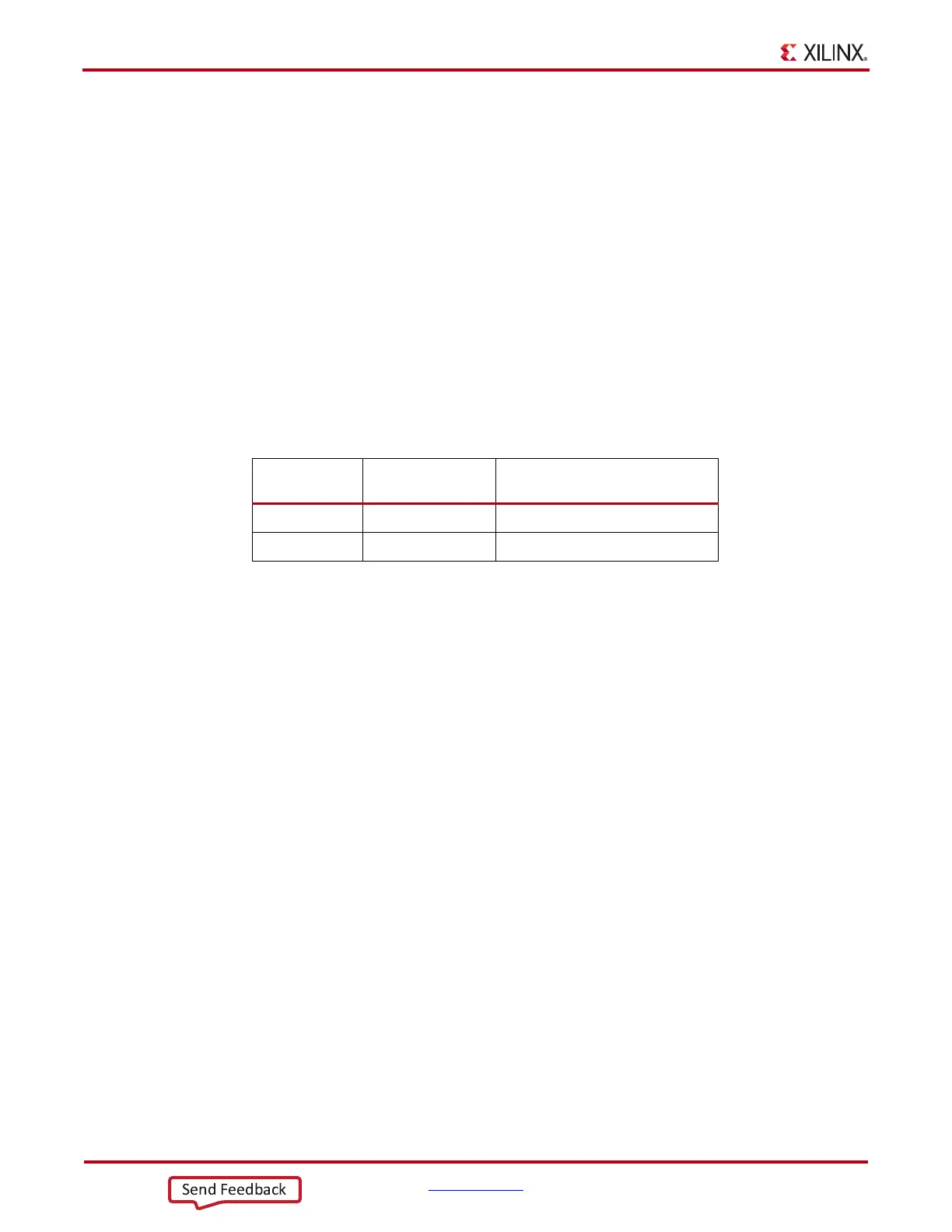
RXUSRCLK2 is the main synchronization clock for all signals into the RX side of the GTP
transceiver. Most signals into the RX side of the GTP transceiver are sampled on the positive edge
of RXUSRCLK2. RXUSRCLK2 and RXUSRCLK have a fixed-rate relationship based on the
RX_DATA_WIDTH setting. Table 4-45 shows the relationship between RXUSRCLK2 and
RXUSRCLK per RX_DATA_WIDTH value.
These rules about the relationships between clocks must be observed for RXUSRCLK and
RXUSRCLK2:
• RXUSRCLK and RXUSRCLK2 must be positive-edge aligned, with as little skew as possible
between them. As a result, low-skew clock resources (BUFGs and BUFHs) should be used to
drive RXUSRCLK and RXUSRCLK2.
• If the channel is configured so the same oscillator drives the reference clock for the transmitter
and the receiver, TXOUTCLK can be used to drive RXUSRCLK and RXUSRCLK2 in the
same way that they are used to drive TXUSRCLK and TXUSRCLK2. When clock correction
is turned off or the RX buffer is bypassed, RX phase alignment must be used to align the serial
clock and the parallel clocks.
• If separate oscillators are driving the reference clocks for the transmitter and receiver on the
channel, and clock correction is not used, RXUSRCLK and RXUSRCLK2 must be driven by
RXOUTCLK (RXOUTCLKSEL = 3'b010 for RXOUTCLKPMA), and the phase-alignment
circuit must be used.
• If clock correction is used, RXUSRCLK and RXUSRCLK2 can be sourced by RXOUTCLK
or TXOUTCLK.
Ports and Attributes
Table 4-46 defines the FPGA RX interface ports.
Table 4-45: RXUSRCLK2 Frequency Relationship to RXUSRCLK
FPGA Interface
Width
RX_DATA_WIDTH RXUSRCLK2 Frequency
2-Byte 16, 20 F
RXUSRCLK2
= F
RXUSRCLK
4-Byte 32, 40 F
RXUSRCLK2
= F
RXUSRCLK
/ 2
RXUSRCLK Rate
Line Rate
Internal Datapath Width
-------------------------------------------------------------------=
 Loading...