232 www.xilinx.com 7 Series FPGAs GTP Transceivers User Guide
UG482 (v1.9) December 19, 2016
Chapter 5: Board Design Guidelines
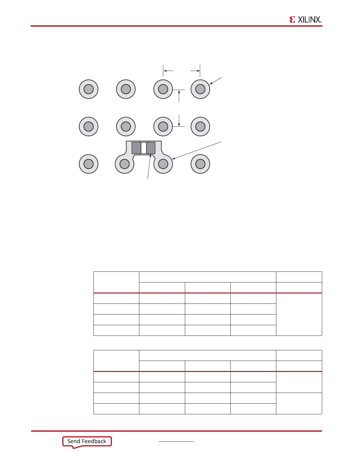
Another choice is to mount an 0201 capacitor next to the BGA via pads. Doing this eliminates the
need to use filled via in pad. An example of this placement is shown in Figure 5-12.
The Artix-7 FPGA and Zynq-7000 AP SoC packages with GTP transceivers have analog power
supply pins and adjacent ground pins. Table 5-8 through Table 5-13 show suggested power and
ground pin pairs for mounting the 0.1 µF capacitors. Following the guidance in these tables and
using the previously discussed layout and placement guidance provides effective power supply
decoupling by maintaining a minimum amount of inductance in the path between the on-die
circuitry and the capacitor on the printed circuit board.
X-Ref Target - Figure 5-12
Figure 5-12: Placement of 0.1 µF 0201 Capacitor on Bottom of PCB Under FPGA
1 mm.
BGA Pin Field Vias
Cover Via With
Solder Mask
0201 Capacitor
1 mm.View From Bottom of PCB
UG482_c5_12_072412
Table 5-8: CLG485 Package – 0.1 µF Capacitor Placement
Capacitor
Package Pins Value
MGTAVCC MGTAVTT GND
Cap1 Y7 W7
0.1 µF
Cap2 AA4 AB4
Cap3 U8 V8
Cap4 W5 Y5
Table 5-9: CPG236 Package – 0.1 µF Capacitor Placement
Capacitor
Package Pins Value
MGTAVCC MGTAVTT GND
Cap1 G7 G8
0.1 µF
Cap2 B1 A1
Cap3 H9 H8
0.1 µF
Cap4 C1 C2
 Loading...