7 Series FPGAs GTP Transceivers User Guide www.xilinx.com 41
UG482 (v1.9) December 19, 2016
Reset and Initialization
PLL Reset
The PLLs (PLL0 and PLL1) must be powered down using the PLL0PD and PLL1PD ports until
reference clock edges are detected in the logic. After PLL0PD/PLL1PD is de-asserted, PLL0 and
PLL1 must be reset before being used. Each GTPE2_COMMON has six dedicated ports for PLL
reset. As shown in Figure 2-12, PLL0RESET is an input that resets PLL0 and PLL1RESET is an
input that resets PLL1. PLL0LOCK and PLL1LOCK are outputs that indicate that the reset process
is done. The guideline for this asynchronous PLL0RESET and PLL1RESET pulse width is one
period of the reference clock. The real PLL0 and PLL1 resets generated by the internal GTP
transceiver circuits are much longer than the PLL0RESET and PLL1RESET High pulse duration.
The time required for the PLL to lock is affected by a few factors, such as bandwidth setting and
clock frequency.
TX Initialization and Reset
The GTP transceiver’s TX uses a reset state machine to control the reset process. The GTP
transceiver’s TX is partitioned into two reset regions, TX PMA and TX PCS. The partition allows
TX initialization and reset to be operated only in sequential mode, as shown in Figure 2-13.
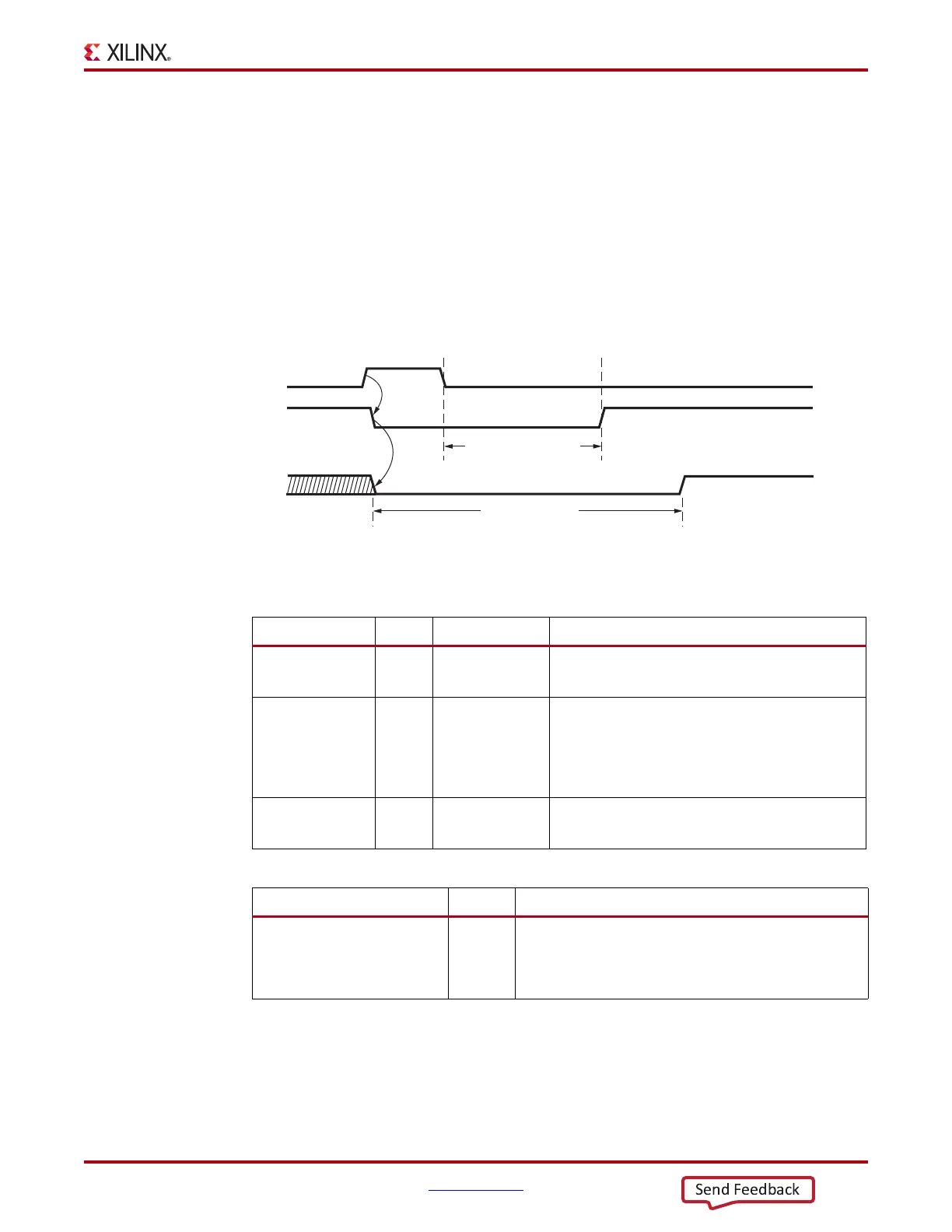
X-Ref Target - Figure 2-12
Figure 2-12: PLL Reset Timing Diagram
PLL0RESET/PLL1RESET
PLL0LOCK/PLL1LOCK
PLL[0/1] Lock Time
PLL[0/1]RESET_TIME
Internal PLL0/PLL1
Reset Signal
(Active Low)
UG482_c2_112_021113
Table 2-12: PLL Reset Port
Port Dir Clock Domain Description
PLL0RESET/
PLL1RESET
In Async This port is driven High and then deasserted to start
the PLL reset.
PLL0LOCK/
PLL1LOCK
Out Async This active-High PLL frequency lock signal
indicates that the PLL frequency is within a
predetermined tolerance. The GTP transceiver and
its clock outputs are not reliable until this condition
is met.
PLL0LOCKEN/
PLL1LOCKEN
In Async This active-High signal enables the PLL lock
detector.
Table 2-13: PLL Reset Attributes
Attribute Type Description
PLL[0/1]RESET_TIME
(PLL[0/1]_INIT_CFG[9:0])
10-bit
Binary
Reserved. Represents the time duration to apply internal
PLL reset. Must be a non-zero value. The recommended
value from the 7 Series FPGAs Transceivers Wizard
should be used.
 Loading...