A-2
A.2 Noise
This section gives a summary of noises generated in inverters and their effects on devices subject to noise.
[ 1 ] Inverter noise
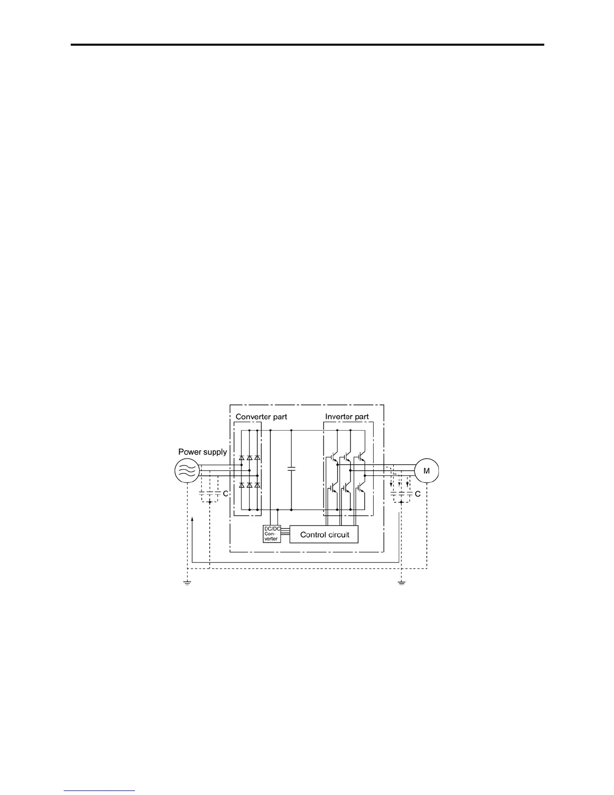
Figure A.1 shows an outline of the inverter configuration. The inverter converts AC to DC (rectification)
in a converter unit, and converts DC to AC (inversion) with 3-phase variable voltage and variable
frequency. The conversion (inversion) is performed by PWM implemented by switching six transistors
(IGBT: Insulated Gate Bipolar Transistor, etc), and is used for variable speed motor control.
Switching noise is generated by high-speed on/off switching of the six transistors. Noise current (i) is
emitted and at each high-speed on/off switching, the noise current flows through stray capacitance (C) of
the inverter, cable and motor to the ground. The amount of the noise current is expressed as follows:
i = C·dv/dt
It is related to the stray capacitance (C) and dv/dt (switching speed of the transistors). Further, this noise
current is related to the carrier frequency since the noise current flows each time the transistors are
switched on or off.
In addition to the main power inverter, the DC-to-DC switching power regulator (DC-DC converter),
which is the power source for the control electronics of the inverter, may be a noise source in the same
principles as stated above.
The frequency band of this noise is less than approximately 30 to 40 MHz. Therefore, the noise will affect
devices such as AM radios using low frequency band, but will not virtually affect FM radios and television
sets using higher frequency than this frequency band.
Figure A.1 Outline of Inverter Configuration
 Loading...