13
1
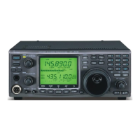
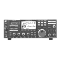
PANEL DESCRIPTION
■ Rear panel (Continued)
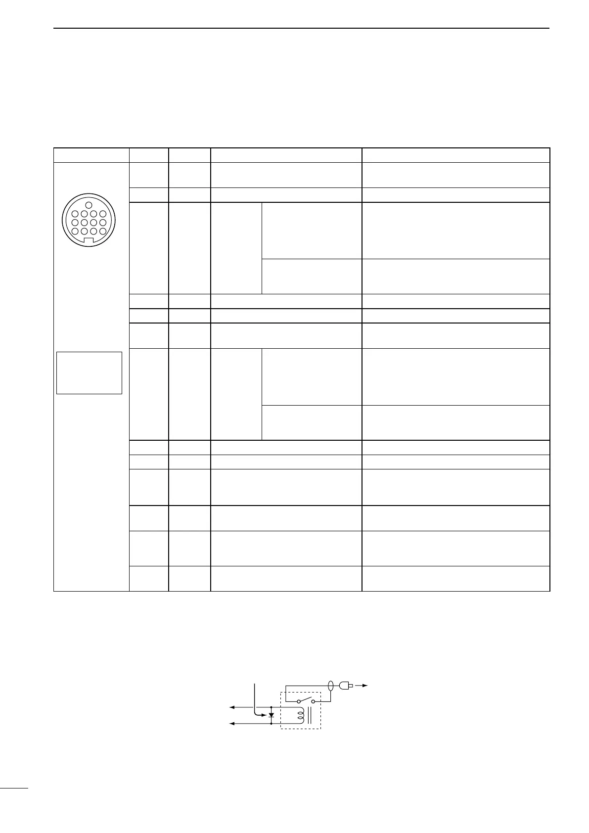
D ACC socket information
• ACC socket
ACC
PIN No.
NAME DESCRIPTION SPECIFICATIONS
1234
8765
9
10 11 12
13
Rear panel view
Color refers to
the cable strands
of the supplied
cable.
q brown
w red
e orange
r yellow
t green
y blue
u purple
i
o
!0
!1
!2
!3
gray
white
black
pink
light
blue
light
green
1 8 V
Regulated 8 V output.
Output voltage
Output current
: 8 V ± 0.3 V
: Less than 10 mA
2 GND
Connects to ground. ———
3
HSEND
*
1, 2
Input/out-
put pin.
An external equipment
controls the transceiver.
When this pin goes low,
the transceiver trans-
mits.
Input voltage (High)
Input voltage (Low)
Current flow
: 2.0 V to 20.0 V
: –0.5 V to +0.8 V
: Max. 20 mA
The transceiver outputs a
low signal to control exter-
nal equipment.
Output voltage (Low)
Current flow
: Less than 0.1 V
: Max. 200 mA
4 NC
——— ———
5 BAND
Band voltage output.
Output voltage : 0 to 8 V
6 ALC
ALC voltage input.
Control voltage
Input impedance
: –3 V to 0 V
: More than 3.3 k˘
7
VSEND
*
1, 2
Input/out-
put pin.
An external equipment
controls the transceiver.
When this pin goes low,
the transceiver trans-
mits.
Input voltage (High)
Input voltage (Low)
Current flow
: 2.0 V to 20.0 V
: –0.5 V to +0.8 V
: Max. 20 mA
The transceiver outputs a
low signal to control exter-
nal equipment.
Output voltage (Low)
Current flow
: Less than 0.1 V
: Max. 200 mA
8 13.8 V
13.8 V output when power is ON.
Output current : Less than 1 A
9 NC ——— ———
10 FSKK
ControlsRTTYkeying
“High” level
“Low” level
Output current
: More than 2.4 V
: Less than 0.6 V
: Less than 2 mA
11 MOD
Modulator input.
Input impedance
Input level
: 10 k˘
: Approx. 100 mV rms
12 AF*
3
AF detector output.
Fixed level, regardless of the [AF]
control position.
Output impedance
Output level
: 4.7 k˘
: 100 to 300 mV rms
13
SQL S*
3
Squelch output.
Grounded when squelch opens.
SQL open
SQL closed
: Less than 0.3 V/5 mA
: More than 6.0 V/100 µA
*
1
When the SEND terminal controls the inductive load (such as a relay), a counter-electromotive force can cause
the transceiver’s malfunction or damage. To prevent this, we recommend adding a switching diode, such as an
“1SS133,” on the load side of the circuit to the counter-electromotive force absorption.
When the diode is added, a switching delay of the relay may occur. Be sure to check its switching action before
operation.
eHSEND or
uVSEND
i13.8 V
ACC socket
Relay
Switching diode
To a non-Icom
linear amplifier
[Example]
*
2
VSEND is used for the 144 MHz, 430 MHz, and 1200 MHz bands, and HSEND is used for the HF/50 MHz bands
bydefault.Youcanchangethissettingin“VSENDSelect”oftheSetmode.(p.166)
*
3
Thepin12(AF)andpin13(SQLS)outputcapabilitiesarefortheMAINBand’sAFandsquelchbydefault.You
can change this setting in “ACC AF/SQL Select” of the Set mode. (p. 166)
 Loading...