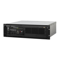
6-1-21. MDC-23 Board
The MDC-23 board mounted in the HKCU-REC55 is a memory board to store 4K/HD video and audio data (for recording
and playback) sent from the camera. The ENC2_FPGA (IC401) controls the following flash memory ICs.
• IC900 to IC903
• IC1000 to IC1003
• IC1100 to IC1103
• IC1200 to IC1203
6-1-22. ENC-185 Board
The ENC-185 board mounted in the HKCU-REC55 is a main processing board to control and process 4K/HD video
and audio signals (for recording, transfer, and playback) sent from the camera.
The FPGA (IC001) has the following functions.
• Controls recording, playback, and transfer with the internal CPU.
• Functions as bank memory (main cache of audio and video data)
• Functions as a host of the MDC-23 board.
• Transfers recording data through the USB Host/10GbE network.
The FPGA (IC001) is connected to eight DDR4 SDRAMs. IC1501 to IC1504 are used as bank memory. C1001 to
IC1004 are used as working memory for the CPU.
Control signals
The storage device communicates with the CPU in the FPGA (IC001) from the LAN-COM connector through the LAN-
HUB (IC403) and is controlled by the CPU.
The CPU (AT-195 board) of the unit is connected to the CPU in the FPGA (IC001) through the CPU_BUS line to transfer
camera settings and alarm information.
Recording processing
The 4K video and audio signals from the camera are input from the TX-167A and TX-167B boards. The HD and audio
signals are input from the VIF-75 board to the FPGA (IC001).
The 4K video signals that are input to the FPGA (IC001) are encoded to 4K XAVC data in IC007. The HD signals are
encoded to HD XAVC data in IC006. These encoded data are returned to the FPGA (IC001).
Encoded video and audio signals and meta data (including time code) are mapped in the FPGA (IC001), and are then
sent to the MDC-23 board using the SATA Host function to be stored in the flash memory on the MDC-23 board.
Playback processing
Recording stream signals are sent from the MDC-23 board to the FPGA (IC001).
The 4K video signals in the recording stream signals are decoded in IC007. The HD signals are decoded in IC006. These
decoded data are returned to the FPGA (IC001) as baseband video signals.
The baseband video and audio signals are mapped to the SDI format in the FPGA (IC001), and are then sent to the
TX-167A, TX-167B, and VIF-75 boards. Then these signals are output as SDI signals from the UHD-SDI B connector
and the SDI I/O 3 connector.
Transfer processing
The recording stream signals sent to the FPGA (IC001) can be transferred to external devices from the USB connector
on the IF-1371 board using the USB Host function (IC001).
In the same way, the recording stream signals can be transferred from the 10GbE network connector through the SFP+
module connected to the CN401 connector using the 10GbE network function of the FPGA (IC001).
HDCU3500/HDCU5500
6-6
 Loading...