7 Series FPGAs GTP Transceivers User Guide www.xilinx.com 165
UG482 (v1.9) December 19, 2016
RX Byte and Word Alignment
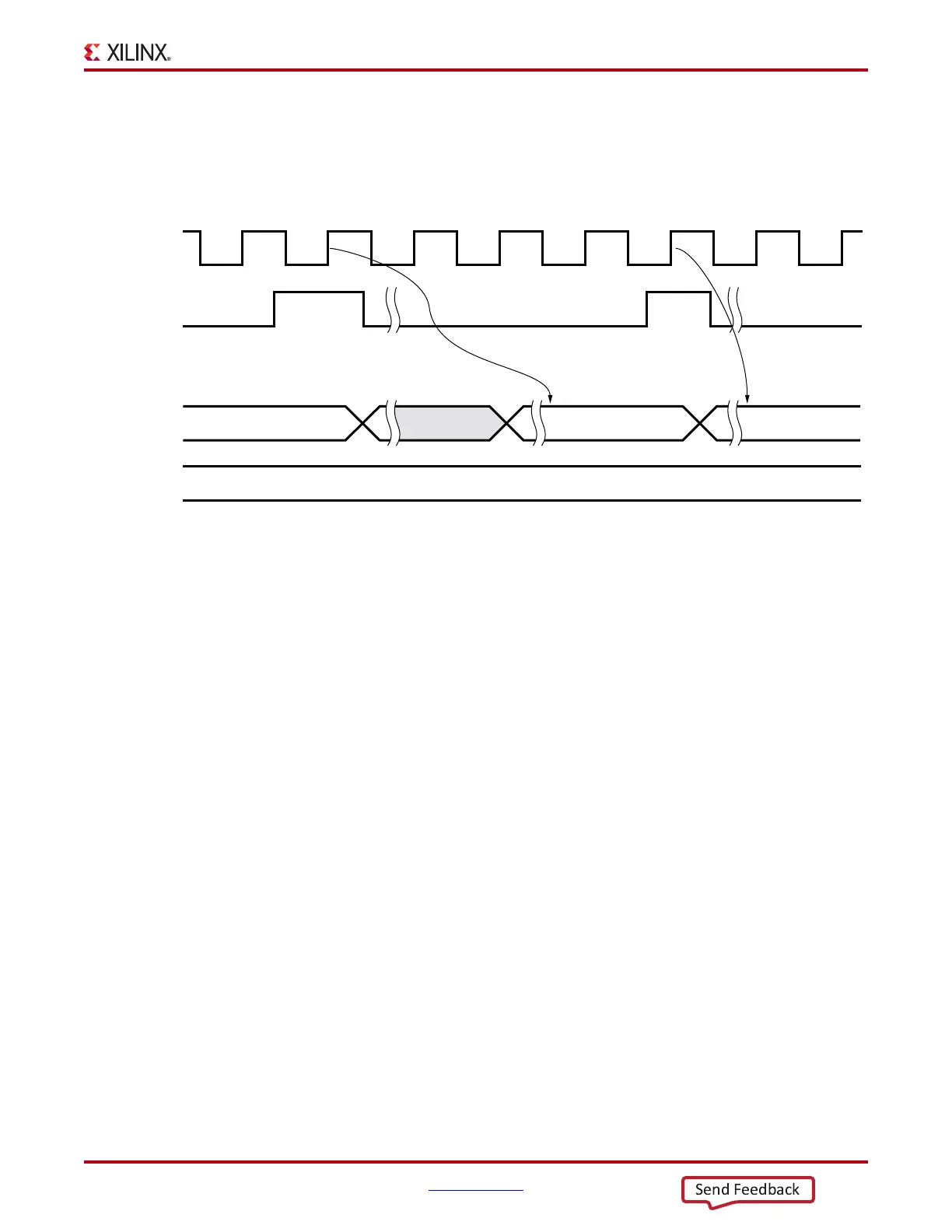
Figure 4-32 shows the waveforms for manual alignment using RXSLIDE in RXSLIDE_MODE =
PMA before and after the data shift. In this mode, the data is shifted right by one bit for every
RXSLIDE pulse issued, but there is some intermediate data with the bits shifted left before the final
data appears on the bus. When RXSLIDE_MODE = PMA is used, the RX recovered clock phase is
shifted by 2 UI for every alternate RXSLIDE pulse.
Note relevant to Figure 4-32:
1. Latency between the slide and the slide result at RXDATA depends on the number of active RX
PCS blocks in the datapath.
X-Ref Target - Figure 4-32
Figure 4-32: Manual Data Alignment Using RXSLIDE for RX_DATA_WIDTH = 20 Bits and
RXSLIDE_MODE = PMA
UG482_c4_21_111011
RXUSRCLK2
RXSLIDE
RXDATA
TXDATA
00000000001001111100
00000000000010011111 10000000000001001111 11000000000000100111
0000000000
0100111110
Intermediate Data
Slide results on RXDATA
after several cycles of latency
through the PCS path
A minimum of 32 RXUSRCLK2
cycles are required between two
RXSLIDE pulses
 Loading...